Datasheet 搜索 > 逻辑控制器 > TI(德州仪器) > SN74LVC2T45DCTTE4 数据手册 > SN74LVC2T45DCTTE4 数据手册 2/25 页
 器件3D模型
¥ 8.336
SN74LVC2T45DCTTE4 数据手册 - TI(德州仪器)
制造商:
TI(德州仪器)
分类:
逻辑控制器
封装:
SSOP-8
描述:
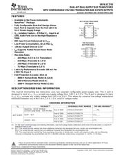
可配置电压转换和三态输出的双位双电源总线收发器 DUAL-BIT DUAL-SUPPLY BUS TRANSCEIVER WITH CONFIGURABLE VOLTAGE TRANSLATION AND 3-STATE OUTPUTS
Pictures:
3D模型
符号图
焊盘图
引脚图
产品图
页面导航:
典型应用电路图在P2
封装尺寸在P17P19P20
型号编码规则在P1P2
标记信息在P1
封装信息在P1P17P18P19P20
功能描述在P15
技术参数、封装参数在P3
应用领域在P18P25
电气规格在P5
导航目录
SN74LVC2T45DCTTE4数据手册
Page:
of 25 Go
若手册格式错乱,请下载阅览PDF原文件
www.ti.com
DESCRIPTION/ORDERING INFORMATION (CONTINUED)
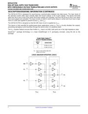
B1
DIR
5
7
A1
2
V
CCA
V
CCB
B2
6
A2
3
SN74LVC2T45
DUAL-BIT DUAL-SUPPLY BUS TRANSCEIVER
WITH CONFIGURABLE VOLTAGE TRANSLATION AND 3-STATE OUTPUTS
SCES516I – DECEMBER 2003 – REVISED MARCH 2007
The SN74LVC2T45 is designed for asynchronous communication between two data buses. The logic levels of
the direction-control (DIR) input activate either the B-port outputs or the A-port outputs. The device transmits
data from the A bus to the B bus when the B-port outputs are activated, and from the B bus to the A bus when
the A-port outputs are activated. The input circuitry on both A and B ports always is active and must have a logic
HIGH or LOW level applied to prevent excess I
CC
and I
CCZ
.
The SN74LVC2T45 is designed so that the DIR input circuit is supplied by V
CCA
.
This device is fully specified for partial-power-down applications using I
off
. The I
off
circuitry disables the outputs,
preventing damaging current backflow through the device when it is powered down.
The V
CC
isolation feature ensures that if either V
CC
input is at GND, both ports are in the high-impedance state.
NanoFree™ package technology is a major breakthrough in IC packaging concepts, using the die as the
package.
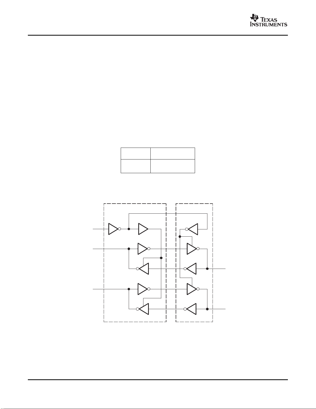
FUNCTION TABLE
(1)
(EACH TRANSCEIVER)
INPUT
OPERATION
DIR
L B data to A bus
H A data to B bus
(1) Input circuits of the data I/Os
always are active.
LOGIC DIAGRAM (POSITIVE LOGIC)
2
Submit Documentation Feedback
器件 Datasheet 文档搜索
AiEMA 数据库涵盖高达 72,405,303 个元件的数据手册,每天更新 5,000 多个 PDF 文件
