Datasheet 搜索 > Flash芯片 > Silicon Storage Tech > SST25VF512A-33-4C-SAE 数据手册 > SST25VF512A-33-4C-SAE 数据手册 3/25 页
 器件3D模型
¥ 0
SST25VF512A-33-4C-SAE 数据手册 - Silicon Storage Tech
制造商:
Silicon Storage Tech
分类:
Flash芯片
封装:
SOIC
Pictures:
3D模型
符号图
焊盘图
引脚图
产品图
页面导航:
引脚图在P3Hot
原理图在P2
型号编码规则在P23
封装信息在P24
导航目录
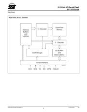
SST25VF512A-33-4C-SAE数据手册
Page:
of 25 Go
若手册格式错乱,请下载阅览PDF原文件
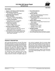
Data Sheet
512 Kbit SPI Serial Flash
SST25VF512A
3
©2006 Silicon Storage Technology, Inc. S71264-02-000 1/06
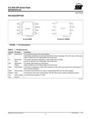
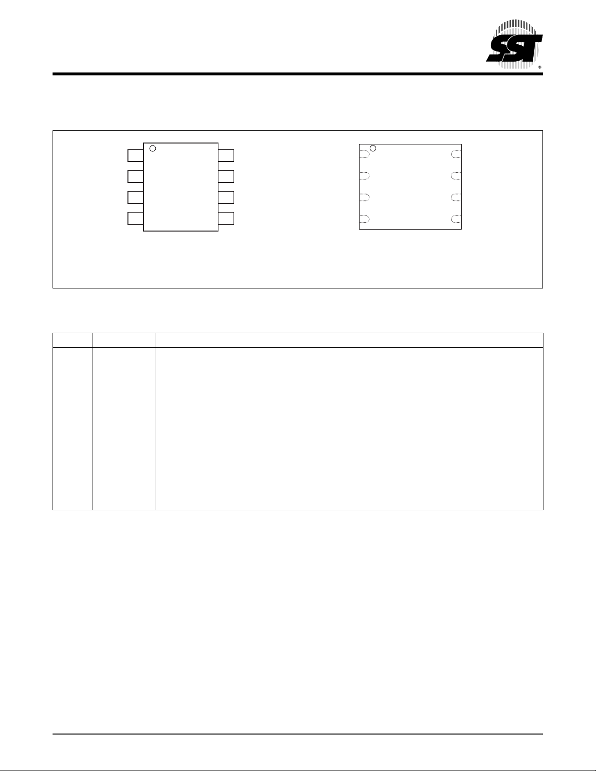
PIN DESCRIPTION
FIGURE 1: PIN ASSIGNMENTS
TABLE 1: PIN DESCRIPTION
Symbol Pin Name Functions
SCK Serial Clock To provide the timing of the serial interface.
Commands, addresses, or input data are latched on the rising edge of the clock input, while output
data is shifted out on the falling edge of the clock input.
SI Serial Data
Input
To transfer commands, addresses, or data serially into the device.
Inputs are latched on the rising edge of the serial clock.
SO Serial Data
Output
To transfer data serially out of the device.
Data is shifted out on the falling edge of the serial clock.
CE# Chip Enable The device is enabled by a high to low transition on CE#. CE# must remain low for the duration of
any command sequence.
WP# Write Protect The Write Protect (WP#) pin is used to enable/disable BPL bit in the status register.
HOLD# Hold To temporarily stop serial communication with SPI flash memory without resetting the device.
V
DD
Power Supply To provide power supply (2.7-3.6V).
V
SS
Ground
T1.0 1264
1
2
3
4
8
7
6
5
CE#
SO
WP#
V
SS
V
DD
HOLD#
SCK
SI
Top View
1264 08-soic P1.0
8-LEAD SOIC 8-CONTACT WSON
1
2
3
4
8
7
6
5
CE#
SO
WP#
V
SS
Top View
V
DD
HOLD#
SCK
SI
1264 08-wson P2.0
器件 Datasheet 文档搜索
AiEMA 数据库涵盖高达 72,405,303 个元件的数据手册,每天更新 5,000 多个 PDF 文件
