Datasheet 搜索 > RS485控制器 > ST Microelectronics(意法半导体) > ST3485EIDT 数据手册 > ST3485EIDT 数据手册 6/22 页

 器件3D模型
¥ 8.045
ST3485EIDT 数据手册 - ST Microelectronics(意法半导体)
制造商:
ST Microelectronics(意法半导体)
分类:
RS485控制器
封装:
SO-8
描述:
RS422/RS485收发器, 1驱动器, 1接收器, 3V至3.6V电源, SOIC-8
Pictures:
3D模型
符号图
焊盘图
引脚图
产品图
页面导航:

导航目录
ST3485EIDT数据手册
Page:
of 22 Go
若手册格式错乱,请下载阅览PDF原文件
Electrical characteristics
ST3485EB, ST3485EC, ST3485EI, ST3485EIY
6/22
DocID9102 Rev 10
4 Electrical characteristics
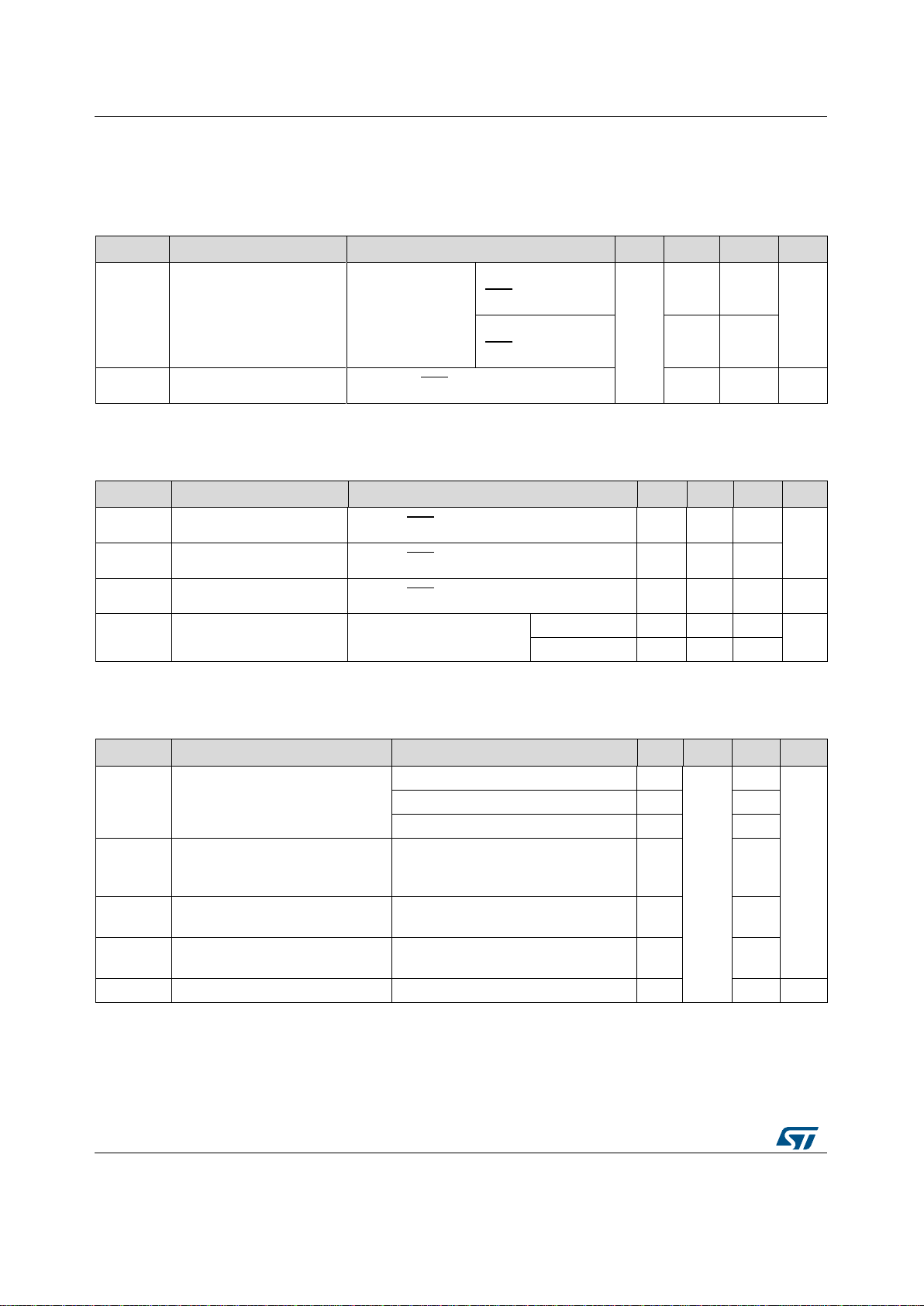
Table 6: Electrical characteristics (VCC = 3 V to 3.6 V, TA = 0 to 70 °C for ST3485ECDR,
TA = -40 to 85 °C for ST3485EBDR, TA = -40 to 125 °C for ST3485EIDT and ST3485EIYDT,
unless otherwise specified. Typical values are referred to TA = 25 °C)
Symbol
Parameter
Test conditions
Min.
Typ.
Max.
Unit
I
SUPPLY
V
CC
power supply current
No load,
DI = 0 V or V
CC
DE = V
CC
,
RE = 0 V or V
CC
—
1.3
2.2
mA
DE = 0 V,
RE = 0 V
1.2
1.9
I
SHDN
Shutdown supply current
DE = 0 V, RE = V
CC
, DI = 0 V or V
CC
0.002
1
µA
Table 7: Logic input electrical characteristics (VCC = 3 V to 3.6 V, TA = 0 to 70 °C for
ST3485ECDR, TA = -40 to 85 °C for ST3485EBDR, TA = -40 to 125 °C for ST3485EIDT and
ST3485EIYDT, unless otherwise specified. Typical values are referred to TA = 25 °C)
Symbol
Parameter
Test conditions
Min.
Typ.
Max.
Unit
V
IL
Input logic threshold low
DE, DI, RE
1.3
0.8
V
V
IH
Input logic threshold high
DE, DI, RE
2
I
IN1
Logic input current
DE, DI, RE
±2.0
µA
I
IN2
Input current (A, B)
DE = 0 V, V
CC
= 0 or 3.6 V
V
IN
= 12 V
1
mA
V
IN
= -7 V
-0.8
Table 8: Transmitter electrical characteristics (VCC = 3 V to 3.6 V, TA = 0 to 70 °C for
ST3485ECDR, TA = -40 to 85 °C for ST3485EBDR, TA = -40 to 125 °C for ST3485EIDT and
ST3485EIYDT, unless otherwise specified. Typical values are referred to TA = 25 °C)
Symbol
Parameter
Test conditions
Min.
Typ.
Max.
Unit
V
OD
Differential drive output
R
L
= 100 Ω (RS-422) (Figure 2)
2
—
V
R
L
= 54 Ω (RS-485) (Figure 2)
1.5
R
L
= 60 Ω (RS-485) (Figure 3)
1.5
∆V
OD
Change in magnitude of driver
differential output voltage for
complementary output states
(1)
R
L
= 54 Ω or 100 Ω (Figure 2)
0.2
V
OC
Driver common mode output
voltage
R
L
= 54 Ω or 100 Ω (Figure 2)
3
∆V
OC
Change in magnitude of driver
common mode output voltage
(1)
R
L
= 54 Ω or 100 Ω (Figure 2)
0.2
I
OSD
Driver short-circuit output current
±250
mA
Notes:
(1)
∆V
OD
and ∆V
OC
are the changes in V
OD
and V
OC
, respectively, when the DI input changes state.
器件 Datasheet 文档搜索
AiEMA 数据库涵盖高达 72,405,303 个元件的数据手册,每天更新 5,000 多个 PDF 文件
