Datasheet 搜索 > 微控制器 > ST Microelectronics(意法半导体) > STM32F303VET6 数据手册 > STM32F303VET6 数据手册 1/184 页
 器件3D模型
¥ 21.182
STM32F303VET6 数据手册 - ST Microelectronics(意法半导体)
制造商:
ST Microelectronics(意法半导体)
分类:
微控制器
封装:
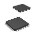
LQFP-100
描述:
STM32F373/383 系列微处理器,STMicroelectronicsSTMicroelectronics ARM® Cortex™ **STM32 F373/383** 系列混合信号微控制器用于嵌入式应用。 **STM32 F3** 系列 32 位闪存 MCU 具有数字信号处理 (DSP) 和浮点单元 (FPU),带高性能和工业标准芯体系。 结合在 72MHz 频率范围内运行的 32 位 ARM® Cortex™ M4 芯,其中具有很多集成的外设(包括 RTC、温度传感器和电容性触摸传感)。 **STM32F373/383** 16 位 sigma delta ADC 用于智能计量和生物识别传感器应用中的高精度传感。 CCM 体系也用于 RAM,用户可以执行对计时关键的程序。 **STM32 F373/383 功能**: 浮点单元 (FPU)、存储器保护装置 (MPU) 和嵌入式追踪 macrocell (ETM) 闪存:高达 256 Kb SRAM:高达 32 Kb 通信接口:I2C、SPI、I2S、USART 和 CAN 芯:ARM® 32 位 Cortex™ M4 CPU(最大值 72MHz) 快速/超快速比较器 运算放大器带可编程增益 (PGA) 12 位 DAC、带 5 MSPS 的 12 位 ADC 电动机控制计时器 (144MHz) CCM(核心耦合存储器) 2.0 至 3.6 V 操作 温度范围 -40 至 +85°C ### STM32F3 系列 32 位 ARM® Cortex®-M4 微控制器,STMicroelectronicsSTM32 F3 系列混合信号 MCU,带有 DSP 和 FPU 指令,将以 72MHz 运行的 32 位 ARM Cortex-M4 内核与高级模拟外设组件组合在一起。快速比较器 (50ns) 可编程增益放大器(4 种增益范围) 12 位 DAC 快速 12 位 ADC(每通道 5 MSPS,交错模式时高达 18 MSPS) 16 位 sigma-delta ADC 快速 144MHz 电动机控制计时器,计时分辨率优于 7ns展开
Pictures:
3D模型
符号图
焊盘图
引脚图
产品图
页面导航:
引脚图在P35P36P37P38P39P40P41P42P43P44P45P46Hot
典型应用电路图在P93P95P154
封装尺寸在P162P163P164P165P166P167P168P169P170P171P172P173
型号编码规则在P179P180P182
技术参数、封装参数在P71
电气规格在P68P69P70P71P72P73P74P75P76P77P78P79
导航目录
STM32F303VET6数据手册
Page:
of 184 Go
若手册格式错乱,请下载阅览PDF原文件
This is information on a product in full production.
December 2015 DocID026415 Rev 4 1/184
STM32F303xD STM32F303xE
ARM
®
Cortex
®
-M4 32b MCU+FPU, up to 512KB Flash, 80KB
SRAM, FSMC, 4 ADCs, 2 DAC ch., 7 comp, 4 Op-Amp, 2.0-3.6 V
Datasheet - production data
Features
• Core: ARM
®
Cortex
®
-M4 32-bit CPU with
72 MHz FPU, single-cycle multiplication and
HW division, 90 DMIPS (from CCM), DSP
instruction and MPU (memory protection unit)
• Operating conditions:
–V
DD
, V
DDA
voltage range: 2.0 V to 3.6 V
• Memories
– Up to 512 Kbytes of Flash memory
– 64 Kbytes of SRAM, with HW parity check
implemented on the first 32 Kbytes.
– Routine booster: 16 Kbytes of SRAM on
instruction and data bus, with HW parity
check (CCM)
– Flexible memory controller (FSMC) for static
memories, with four Chip Select
• CRC calculation unit
• Reset and supply management
– Power-on/Power-down reset (POR/PDR)
– Programmable voltage detector (PVD)
– Low power modes: Sleep, Stop and Standby
–V
BAT
supply for RTC and backup registers
• Clock management
–4
to 32 MHz crystal oscillator
– 32 kHz oscillator for RTC with calibration
– Internal 8 MHz RC with x 16 PLL option
– Internal 40 kHz oscillator
• Up to 115 fast I/Os
– All mappable on external interrupt vectors
– Several 5 V-tolerant
• Interconnect matrix
• 12-channel DMA controller
• Four ADCs 0.20 µs (up to 40 channels) with
selectable resolution of 12/10/8/6 bits, 0 to
3.6 V conversion range, separate analog
supply from 2.0 to 3.6 V
• Two 12-bit DAC channels with analog supply
from 2.4 to 3.6 V
• Seven ultra-fast rail-to-rail analog comparators
with analog supply from 2.0 to 3.6 V
• Four operational amplifiers that can be used in
PGA mode, all terminals accessible with analog
supply from 2.4 to 3.6 V
•
Up to 24 capacitive sensing channels supporting
touchkey, linear and rotary touch sensor
s
• Up to 14 timers
– One 32-bit timer and two 16-bit timers with
up to four IC/OC/PWM or pulse counter and
quadrature (incremental) encoder input
– Three 16-bit 6-channel advanced-control
timers, with up to six PWM channels,
deadtime generation and emergency stop
– One 16-bit timer with two IC/OCs, one
OCN/PWM, deadtime generation and
emergency stop
– Two 16-bit timers with IC/OC/OCN/PWM,
deadtime generation and emergency stop
– Two watchdog timers (independent, window)
– One SysTick timer: 24-bit downcounter
– Two 16-bit basic timers to drive the DAC
• Calendar RTC with Alarm, periodic wakeup
from Stop/Standby
• Communication interfaces
– CAN interface (2.0B Active)
– Three I
2
C Fast mode plus (1 Mbit/s) with
20 mA current sink, SMBus/PMBus, wakeup
from STOP
– Up to five USART/UARTs (ISO 7816
interface, LIN, IrDA, modem control)
– Up to four SPIs, 4 to 16 programmable bit
frames, two with multiplexed half/full duplex
I2S interface
– USB 2.0 full speed interface with LPM
support
– Infrared transmitter
• SWD, Cortex
®
-M4 with FPU ETM, JTAG
• 96-bit unique ID
Table 1. Device summary
Reference Part number
STM32F303xD STM32F303RD, STM32F303VD, STM32F303ZD.
STM32F303xE STM32F303RE, STM32F303VE, STM32F303ZE.
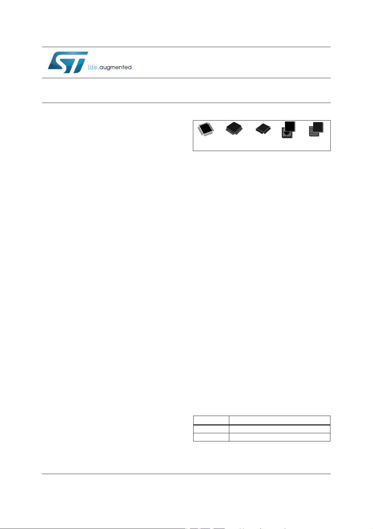
LQFP64
LQFP100
LQFP144
UFBGA100
(10 × 10 mm)
(14 × 14 mm)
(20 x 20 mm)
)%*$
(7 x 7 mm)
WLCSP100
(
4.775 x 5.041 mm
)
www.st.com
器件 Datasheet 文档搜索
AiEMA 数据库涵盖高达 72,405,303 个元件的数据手册,每天更新 5,000 多个 PDF 文件
