Datasheet 搜索 > 微控制器 > ST Microelectronics(意法半导体) > STM32F746VGT7 数据手册 > STM32F746VGT7 数据手册 201/227 页
 器件3D模型
¥ 91.419
STM32F746VGT7 数据手册 - ST Microelectronics(意法半导体)
制造商:
ST Microelectronics(意法半导体)
分类:
微控制器
封装:
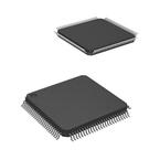
LQFP-100
描述:
ARM Cortex-M7 216MHz 闪存:1MB RAM:320KB
Pictures:
3D模型
符号图
焊盘图
引脚图
产品图
页面导航:
引脚图在P45P46P47P48P49P50P51P52P53P54P55P56Hot
典型应用电路图在P125P126P149
封装尺寸在P196P197P198P199P200P201P202P203P204P205P206P207
型号编码规则在P223
标记信息在P198P201P204P207P211P215P218P221
技术参数、封装参数在P96P137
电气规格在P94P95P96P97P98P99P100P101P102P103P104P105
导航目录
STM32F746VGT7数据手册
Page:
of 227 Go
若手册格式错乱,请下载阅览PDF原文件
DocID027590 Rev 4 201/227
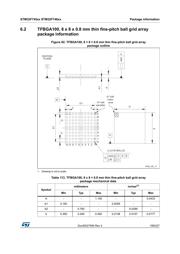
STM32F745xx STM32F746xx Package information
226
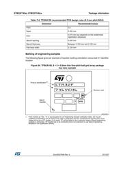
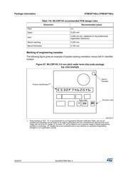
Marking of engineering samples
The following figure gives an example of topside marking orientation versus ball A1 identifier
location.
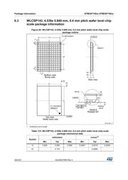
Figure 84. TFBGA100, 8 × 8 × 0.8mm thin fine-pitch ball grid array package
top view example
1. Parts marked as “ES”, “E” or accompanied by an Engineering Sample notification letter, are not yet
qualified and therefore not yet ready to be used in production and any consequences deriving from such
usage will not be at ST charge. In no event, ST will be liable for any customer usage of these engineering
samples in production. ST Quality has to be contacted prior to any decision to use these Engineering
samples to run qualification activity.
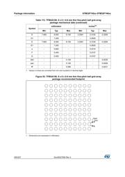
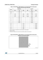
Table 114. TFBGA100 recommended PCB design rules (0.8 mm pitch BGA)
Dimension Recommended values
Pitch 0.8
Dpad 0.400 mm
Dsm
0.470 mm typ (depends on the soldermask
registration tolerance)
Stencil opening 0.400 mm
Stencil thickness Between 0.100 mm and 0.125 mm
Pad trace width 0.120 mm
069
%DOO$
LGHQWLILHU
'DWHFRGH
:88
5HYLVLRQFRGH
3URGXFWLGHQWLILFDWLRQ
3
45.'
7()
器件 Datasheet 文档搜索
AiEMA 数据库涵盖高达 72,405,303 个元件的数据手册,每天更新 5,000 多个 PDF 文件
