Datasheet 搜索 > 齐纳二极管 > ON Semiconductor(安森美) > SZ1SMA5919BT3G 数据手册 > SZ1SMA5919BT3G 数据手册 1/5 页

¥ 2.07
SZ1SMA5919BT3G 数据手册 - ON Semiconductor(安森美)
制造商:
ON Semiconductor(安森美)
分类:
齐纳二极管
封装:
DO-214AC
描述:
SZ1SMA5919BT3G 编带
Pictures:
3D模型
符号图
焊盘图
引脚图
产品图
页面导航:
导航目录
SZ1SMA5919BT3G数据手册
Page:
of 5 Go
若手册格式错乱,请下载阅览PDF原文件
© Semiconductor Components Industries, LLC, 2016
April, 2016 − Rev. 9
1 Publication Order Number:
1SMA5913BT3/D
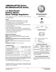
1SMA59xxBT3G Series,
SZ1SMA59xxBT3G Series
1.5 Watt Plastic
Surface Mount
Zener Voltage Regulators
This complete new line of 1.5 Watt Zener Diodes offers the
following advantages.
Features
• Standard Zener Breakdown Voltage Range − 3.3 V to 68 V
• ESD Rating of Class 3 (> 16 kV) per Human Body Model
• Flat Handling Surface for Accurate Placement
• Package Design for Top Slide or Bottom Circuit Board Mounting
• Low Profile Package
• Ideal Replacement for MELF Packages
• AEC−Q101 Qualified and PPAP Capable − SZ1SMA59xxBT3G
• SZ Prefix for Automotive and Other Applications Requiring Unique
Site and Control Change Requirements
• These are Pb−Free Devices*
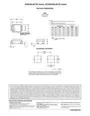
Mechanical Characteristics:
CASE:
Void-free, transfer-molded plastic
FINISH: All external surfaces are corrosion resistant with readily
solderable leads
MAXIMUM CASE TEMPERATURE FOR SOLDERING PURPOSES:
260°C for 10 seconds
POLARITY: Cathode indicated by molded polarity notch or cathode
band
FLAMMABILITY RATING: UL 94 V−0 @ 0.125 in
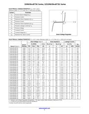
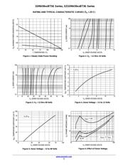
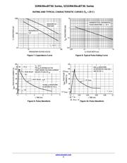
MAXIMUM RATINGS
Rating Symbol Value Unit
DC Power Dissipation @ T
L
= 75°C,
Measured Zero Lead Length (Note 1)
Derate above 75°C
Thermal Resistance, Junction−to−Lead
P
D
R
q
JL
1.5
20
50
W
mW/°C
°C/W
DC Power Dissipation @ T
A
= 25°C (Note 2)
Derate above 25°C
Thermal Resistance, Junction−to−Ambient
P
D
R
q
JA
0.5
4.0
250
W
mW/°C
°C/W
Operating and Storage Temperature Range T
J
, T
stg
−65 to
+150
°C
Stresses exceeding those listed in the Maximum Ratings table may damage the
device. If any of these limits are exceeded, device functionality should not be
assumed, damage may occur and reliability may be affected.
1. 1 in square copper pad, FR−4 board.
2. FR−4 Board, using ON Semiconductor minimum recommended footprint.
*For additional information on our Pb−Free strategy and soldering details, please
download the ON Semiconductor Soldering and Mounting Techniques
Reference Manual, SOLDERRM/D.
CATHODE ANODE
Device Package Shipping
†
ORDERING INFORMATION
www.
onsemi.com
1SMA59xxBT3G SMA
(Pb−Free)
5,000 /
Tape & Reel
†For information on tape and reel specifications,
including part orientation and tape sizes, please
refer to our Tape and Reel Packaging Specifications
Brochure, BRD8011/D.
SMA
CASE 403D
STYLE 1
MARKING DIAGRAM
8xxB
AYWWG
8xxB = Device Code (Refer to page 2)
A = Assembly Location
Y = Year
WW = Work Week
G = Pb−Free Package
See specific marking information in the device marking
column of the Electrical Characteristics table on page 2 o
f
this data sheet.
DEVICE MARKING INFORMATION
SZ1SMA59xxBT3G SMA
(Pb−Free)
5,000 /
Tape & Reel
器件 Datasheet 文档搜索
AiEMA 数据库涵盖高达 72,405,303 个元件的数据手册,每天更新 5,000 多个 PDF 文件
