Datasheet 搜索 > FET驱动器 > Microchip(微芯) > TC4424VMF713 数据手册 > TC4424VMF713 数据手册 3/20 页
 器件3D模型
¥ 13.294
TC4424VMF713 数据手册 - Microchip(微芯)
制造商:
Microchip(微芯)
分类:
FET驱动器
封装:
DFN-8
描述:
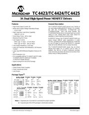
3A双高速功率MOSFET驱动器 3A Dual High-Speed Power MOSFET Drivers
Pictures:
3D模型
符号图
焊盘图
引脚图
产品图
页面导航:
导航目录
TC4424VMF713数据手册
Page:
of 20 Go
若手册格式错乱,请下载阅览PDF原文件
2002-2012 Microchip Technology Inc. DS21421E-page 3
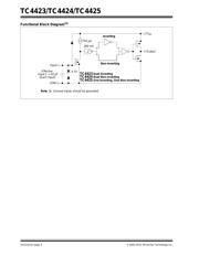
TC4423/TC4424/TC4425
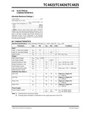
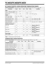
1.0 ELECTRICAL
CHARACTERISTICS
Absolute Maximum Ratings †
Supply Voltage................................................................+22V
Input Voltage, IN A or IN B
................................................(V
DD
+ 0.3V) to (GND – 5V)
Package Power Dissipation (T
A
70°C)
DFN......................................................................... Note 2
PDIP.......................................................................730 mW
SOIC.......................................................................470 mW
† Notice: Stresses above those listed under "Maximum
Ratings" may cause permanent damage to the device. This is
a stress rating only and functional operation of the device at
those or any other conditions above those indicated in the
operational sections of this specification is not intended.
Exposure to maximum rating conditions for extended periods
may affect device reliability.
DC CHARACTERISTICS
Electrical Specifications: Unless otherwise indicated, T
A
= +25°C, with 4.5V V
DD
18V.
Parameters Sym Min Typ Max Units Conditions
Input
Logic ‘1’, High Input Voltage V
IH
2.4 — — V
Logic ‘0’, Low Input Voltage V
IL
——0.8V
Input Current I
IN
–1 — 1 µA 0VV
IN
V
DD
Output
High Output Voltage V
OH
V
DD
– 0.025 — — V
Low Output Voltage V
OL
— — 0.025 V
Output Resistance, High R
OH
—2.85 I
OUT
= 10 mA, V
DD
= 18V
Output Resistance, Low R
OL
—3.55 I
OUT
= 10 mA, V
DD
= 18V
Peak Output Current I
PK
—3—A
Latch-Up Protection With-
stand Reverse Current
I
REV
— >1.5 — A Duty cycle2%, t 300 µsec.
Switching Time (Note 1)
Rise Time t
R
—2335nsFigure 4-1, Figure 4-2,
C
L
= 1800 pF
Fall Time t
F
—2535nsFigure 4-1, Figure 4-2,
C
L
= 1800 pF
Delay Time t
D1
—3375nsFigure 4-1, Figure 4-2,
C
L
= 1800 pF
Delay Time t
D2
—3875nsFigure 4-1, Figure 4-2,
C
L
= 1800 pF
Power Supply
Power Supply Current I
S
—
—
1.5
0.15
2.5
0.25
mA V
IN
= 3V (Both inputs)
V
IN
= 0V (Both inputs)
Note 1: Switching times ensured by design.
2: Package power dissipation is dependent on the copper pad area on the PCB.
器件 Datasheet 文档搜索
AiEMA 数据库涵盖高达 72,405,303 个元件的数据手册,每天更新 5,000 多个 PDF 文件
