Datasheet 搜索 > 接口芯片 > TI(德州仪器) > TCA6408APWR 数据手册 > TCA6408APWR 数据手册 4/44 页
 器件3D模型
¥ 1.998
TCA6408APWR 数据手册 - TI(德州仪器)
制造商:
TI(德州仪器)
分类:
接口芯片
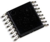
封装:
TSSOP-16
描述:
TEXAS INSTRUMENTS TCA6408APWR 输入/输出扩展, 8bit, 400 kHz, I2C, 1.65 V, 5.5 V, TSSOP
Pictures:
3D模型
符号图
焊盘图
引脚图
产品图
页面导航:
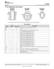
引脚图在P3Hot
典型应用电路图在P16P26
原理图在P1P16P17P26
封装尺寸在P33P35P36
标记信息在P33
封装信息在P32P33P34P35P36
技术参数、封装参数在P4
应用领域在P1P25P44
电气规格在P6P27
导航目录
TCA6408APWR数据手册
Page:
of 44 Go
若手册格式错乱,请下载阅览PDF原文件
TCA6408A
SCPS192D –APRIL 2009–REVISED JULY 2015
www.ti.com
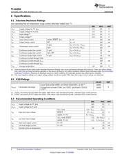
6 Specifications
6.1 Absolute Maximum Ratings
over operating free-air temperature range (unless otherwise noted) (see
(1)
)
MIN MAX UNIT
V
CCI
Supply voltage for I
2
C pins –0.5 6.5 V
V
CCP
Supply voltage for P-ports –0.5 6.5 V
V
I
Input voltage
(2)
–0.5 6.5 V
V
O
Output voltage
(2)
–0.5 6.5 V
I
IK
Input clamp current ADDR, RESET, SCL V
I
< 0 ±20 mA
I
OK
Output clamp current INT V
O
< 0 ±20 mA
P-port V
O
< 0 or V
O
> V
CCP
±20
I
IOK
Input/output clamp current mA
SDA V
O
< 0 or V
O
> V
CCI
±20
Continuous output low current P-port V
O
= 0 to V
CCP
50
I
OL
mA
Continuous output low current SDA, INT V
O
= 0 to V
CCI
25
I
OH
Continuous output high current P-port V
O
= 0 to V
CCP
50 mA
Continuous current through GND 200
I
CC
Continuous current through V
CCP
160 mA
Continuous current through V
CCI
10
T
stg
Storage temperature –65 150 °C
(1) Stresses beyond those listed under Absolute Maximum Ratings may cause permanent damage to the device. These are stress ratings
only, which do not imply functional operation of the device at these or any other conditions beyond those indicated under Recommended
Operating Conditions. Exposure to absolute-maximum-rated conditions for extended periods may affect device reliability.
(2) The input negative-voltage and output voltage ratings may be exceeded if the input and output current ratings are observed.
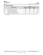
6.2 ESD Ratings
VALUE UNIT
Human body model (HBM), per ANSI/ESDA/JEDEC JS-001
(1)
±2000
V
(ESD)
Electrostatic discharge V
Charged-device model (CDM), per JEDEC specification JESD22- ±1000
C101
(2)
(1) JEDEC document JEP155 states that 500-V HBM allows safe manufacturing with a standard ESD control process.
(2) JEDEC document JEP157 states that 250-V CDM allows safe manufacturing with a standard ESD control process.
6.3 Recommended Operating Conditions
MIN MAX UNIT
V
CCI
Supply voltage for I
2
C pins 1.65 5.5 V
V
CCP
Supply voltage for P-ports 1.65 5.5
SCL, SDA 0.7 × V
CCI
V
CCI
V
IH
High-level input voltage RESET 0.7 × V
CCI
5.5 V
ADDR, P7–P0 0.7 × V
CCP
5.5
SCL, SDA, RESET –0.5 0.3 × V
CCI
V
IL
Low-level input voltage V
ADDR, P7–P0 –0.5 0.3 × V
CCP
I
OH
High-level output current P7–P0 10 mA
I
OL
Low-level output current P7–P0 25 mA
T
A
Operating free-air temperature –40 85 °C
4 Submit Documentation Feedback Copyright © 2009–2015, Texas Instruments Incorporated
Product Folder Links: TCA6408A
器件 Datasheet 文档搜索
AiEMA 数据库涵盖高达 72,405,303 个元件的数据手册,每天更新 5,000 多个 PDF 文件
