Datasheet 搜索 > 逻辑控制器 > TI(德州仪器) > TCA9546APWR 数据手册 > TCA9546APWR 数据手册 16/30 页

 器件3D模型
¥ 2.515
TCA9546APWR 数据手册 - TI(德州仪器)
制造商:
TI(德州仪器)
分类:
逻辑控制器
封装:
TSSOP-16
描述:
TCA9546APWR 编带
Pictures:
3D模型
符号图
焊盘图
引脚图
产品图
页面导航:
引脚图在P3Hot
典型应用电路图在P16P17P18
原理图在P10P16
封装尺寸在P23P25P26
标记信息在P23
封装信息在P22P23P24P25P26
技术参数、封装参数在P4
应用领域在P1P16
电气规格在P5P6P17
导航目录
TCA9546APWR数据手册
Page:
of 30 Go
若手册格式错乱,请下载阅览PDF原文件
TCA9546A
SD1
SDA
Channel 0
Channel 1
Channel 2
Channel 3
I
2
C/SMBus
Master
SCL
RESET
SC1
SD2
SC2
SD3
SC3
SD0
SC0
V
DPUM
= 1.65 V to 5.5 V
V
CC
= 3.3 V
V
DPU0
= 1.65 V to 5.5 V
V = 1.65 V to 5.5 V
DPU1
V = 1.65 V to 5.5 V
DPU2
V = 1.65 V to 5.5 V
DPU3
SDA
SCL
A2
A1
A0
GND
15
14
3
8
1
2
13
16
12
11
10
9
7
6
5
4
VCC
TCA9546A
SCPS205A –APRIL 2014–REVISED FEBRUARY 2015
www.ti.com
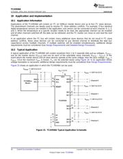
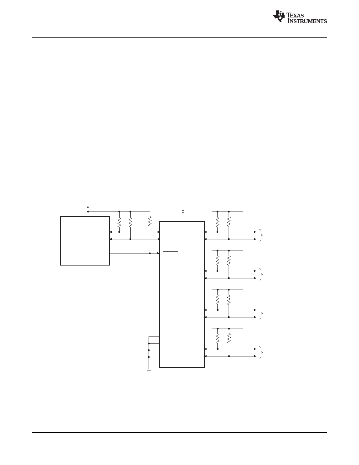
10 Application and Implementation
10.1 Application Information
Applications of the TCA9546A will contain an I
2
C (or SMBus) master device and up to four I
2
C slave devices.
The downstream channels are ideally used to resolve I
2
C slave address conflicts. For example, if four identical
digital temperature sensors are needed in the application, one sensor can be connected at each channel: 0, 1, 2,
and 3. When the temperature at a specific location needs to be read, the appropriate channel can be enabled
and all other channels switched off, the data can be retrieved, and the I
2
C master can move on and read the next
channel.
In an application where the I
2
C bus will contain many additional slave devices that do not result in I
2
C slave
address conflicts, these slave devices can be connected to any desired channel to distribute the total bus
capacitance across multiple channels. If multiple switches will be enabled simultaneously, additional design
requirements must be considered (See Design Requirements and Detailed Design Procedure).
10.2 Typical Application
A typical application of the TCA9546A will contain anywhere from 1 to 5 separate data pull-up voltages, V
DPUX
,
one for the master device (V
DPUM
) and one for each of the selectable slave channels (V
DPU0
– V
DPU3
). In the
event where the master device and all slave devices operate at the same voltage, then the pass voltage, V
pass
=
V
DPUX
. Once the maximum V
pass
is known, V
cc
can be selected easily using Figure 16. In an application where
voltage translation is necessary, additional design requirements must be considered (See Design Requirements).
Figure 15 shows an application in which the TCA9546A can be used.
Figure 15. TCA9546A Typical Application Schematic
16 Submit Documentation Feedback Copyright © 2014–2015, Texas Instruments Incorporated
Product Folder Links: TCA9546A
器件 Datasheet 文档搜索
AiEMA 数据库涵盖高达 72,405,303 个元件的数据手册,每天更新 5,000 多个 PDF 文件
