Datasheet 搜索 > 开发板 > Microchip(微芯) > TCHIP011 数据手册 > TCHIP011 数据手册 165/320 页

¥ 251.277
TCHIP011 数据手册 - Microchip(微芯)
制造商:
Microchip(微芯)
分类:
开发板
描述:
MICROCHIP TCHIP011 评估板, Fubarino Mini ChipKit, 48MHZ PIC32 CPU, 33输入/输出引脚, 兼容Arduino
Pictures:
3D模型
符号图
焊盘图
引脚图
产品图
页面导航:
引脚图在P4P5P6P7P8P9P10P11P12P13P14P20Hot
典型应用电路图在P31
原理图在P19P33P83P87P105P143P151P155P156P159P163P165
封装尺寸在P291P309
标记信息在P289P290P309
封装信息在P246P289P292P294P295P296P299P300P304P305P306P309
功能描述在P37P185
技术参数、封装参数在P218P219P220P247P250P251P253P254P256P274P275P282
电气规格在P28P204P218P219P220P251P282P309P310
导航目录
TCHIP011数据手册
Page:
of 320 Go
若手册格式错乱,请下载阅览PDF原文件

© 2011-2012 Microchip Technology Inc. Preliminary DS61168D-page 165
PIC32MX1XX/2XX
16.0 SERIAL PERIPHERAL
INTERFACE (SPI)
The SPI module is a synchronous serial interface that
is useful for communicating with external peripherals
and other microcontroller devices. These peripheral
devices may be Serial EEPROMs, Shift registers, dis-
play drivers, Analog-to-Digital Converters (ADC), etc.
The PIC32 SPI module is compatible with Motorola
®
SPI and SIOP interfaces.
Some of the key features of the SPI module are:
• Master and Slave modes support
• Four different clock formats
• Enhanced Framed SPI protocol support
• User-configurable 8-bit, 16-bit and 32-bit data width
• Separate SPI FIFO buffers for receive and transmit
- FIFO buffers act as 4/8/16-level deep FIFOs
based on 32/16/8-bit data width
• Programmable interrupt event on every 8-bit,
16-bit and 32-bit data transfer
• Operation during CPU Sleep and Idle mode
• Audio Codec Support:
-I
2
S protocol
- Left-justified
- Right-justified
-PCM
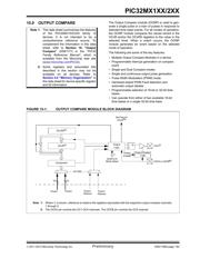
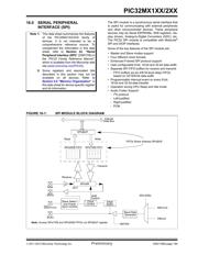
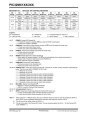
FIGURE 16-1: SPI MODULE BLOCK DIAGRAM
Note 1: This data sheet summarizes the features
of the PIC32MX1XX/2XX family of
devices. It is not intended to be a
comprehensive reference source. To
complement the information in this data
sheet, refer to Section 23. “Serial
Peripheral Interface (SPI)” (DS61106) in
the “PIC32 Family Reference Manual”,
which is available from the Microchip web
site (www.microchip.com/PIC32).
2: Some registers and associated bits
described in this section may not be
available on all devices. Refer to
Section 4.0 “Memory Organization” in
this data sheet for device-specific register
and bit information.
Internal
Data Bus
SDIx
SDOx
SSx
/FSYNC
SCKx
SPIxSR
bit 0
Shift
Control
Edge
Select
MSTEN
Baud Rate
Slave Select
Sync Control
Clock
Control
Transmit
Receive
and Frame
Note: Access SPIxTXB and SPIxRXB FIFOs via SPIxBUF register.
FIFOs Share Address SPIxBUF
SPIxBUF
Generator
PBCLK
WriteRead
SPIxTXB FIFO
SPIxRXB FIFO
REFCLK
MCLKSEL
器件 Datasheet 文档搜索
AiEMA 数据库涵盖高达 72,405,303 个元件的数据手册,每天更新 5,000 多个 PDF 文件
