Datasheet 搜索 > 音频放大器 > ST Microelectronics(意法半导体) > TDA7266D13TR 数据手册 > TDA7266D13TR 数据手册 6/13 页

¥ 10.598
TDA7266D13TR 数据手册 - ST Microelectronics(意法半导体)
制造商:
ST Microelectronics(意法半导体)
分类:
音频放大器
封装:
PowerSO-20
描述:
2声道 立体声 5 W AB类 22引脚 (20+2Tab) PowerSO 卷盘
Pictures:
3D模型
符号图
焊盘图
引脚图
产品图
页面导航:
引脚图在P2Hot
封装尺寸在P7
技术参数、封装参数在P2P13
导航目录
TDA7266D13TR数据手册
Page:
of 13 Go
若手册格式错乱,请下载阅览PDF原文件
TDA7266D
6/13
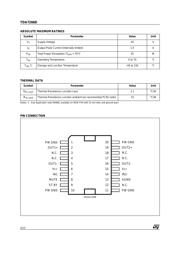
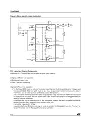
Figure 3. Stand-alone low-cost Application
PCB Layout and External Components:
Regarding the PCB layout care must be taken for three main subjects:
c) Signal and Power Gnd separation
d) Dissipating Copper Area
e) Filter Capacitors positioning
)Signal and Power Gnd separation:
c To the Signal GND must be referred the Audio Input Signals, the Mute and Stand-by Voltages and
the device PIN.13. This Gnd path must be as clean as possible in order to improve the device
THD+Noise and to avoid spurious oscillations across the speakers.
The Power GND is directly connected to the Output power Stage transistors (Emitters) and is crossed
by large amount of current, this path is also used in this device to dissipate the heating generated (no
needs of external heatsinker).
Referring to the typical application circuit, the separation between the two GND paths must be ob-
tained connecting them separately (star routing) to the bulk
Electrolithic capacitor C1 (470µF).
Regarding the Power Gnd dimensioning we have to consider the Dissipated Power the Thermal Pro-
tection Threshold and the Package thermal Characteristics.
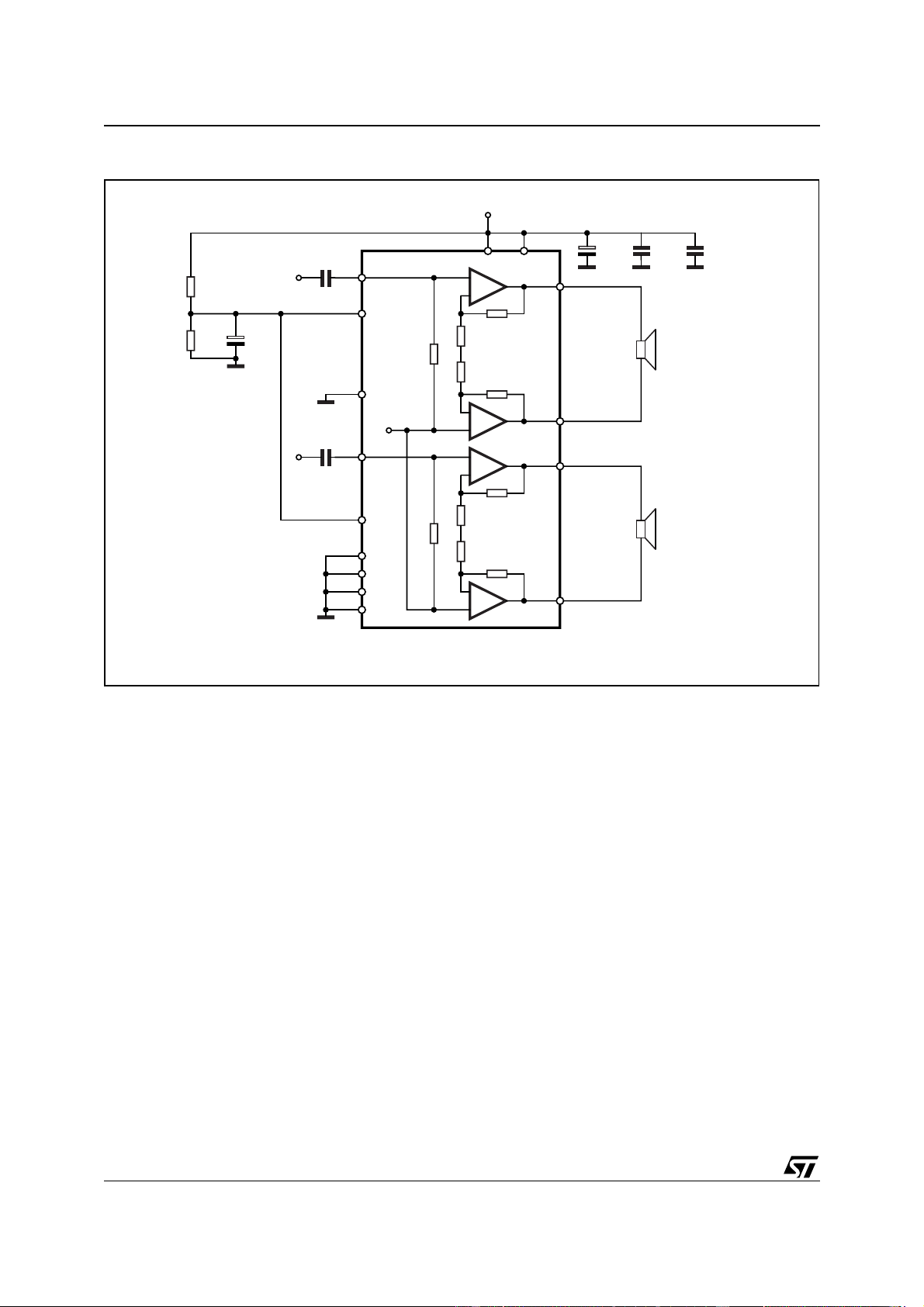
2
5
7
Vref
ST-BY
9
IN1
C3 0.22µF
V
CC
156
D02AU1410
+
-
-
+
OUT1+
OUT1-
19
16
14
MUTE
8
IN2
C5 0.22µF
+
-
-
+
OUT2+
OUT2-
20
13
S-GND
PW-GND
C1
470µF
C2
100nF
C7
100nF
R1
47K
C4
10µF
R2
47K
1
10
11
器件 Datasheet 文档搜索
AiEMA 数据库涵盖高达 72,405,303 个元件的数据手册,每天更新 5,000 多个 PDF 文件
