Datasheet 搜索 > 接口芯片 > NXP(恩智浦) > TJA1028T/3V3/20,118 数据手册 > TJA1028T/3V3/20,118 数据手册 4/24 页

 器件3D模型
¥ 4.197
TJA1028T/3V3/20,118 数据手册 - NXP(恩智浦)
制造商:
NXP(恩智浦)
分类:
接口芯片
封装:
SOIC
Pictures:
3D模型
符号图
焊盘图
引脚图
产品图
页面导航:
导航目录
TJA1028T/3V3/20,118数据手册
Page:
of 24 Go
若手册格式错乱,请下载阅览PDF原文件
TJA1028 All information provided in this document is subject to legal disclaimers. © NXP B.V. 2012. All rights reserved.
Product data sheet Rev. 4 — 25 July 2012 4 of 24
NXP Semiconductors
TJA1028
LIN transceiver with integrated voltage regulator
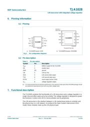
6. Pinning information
6.1 Pinning
6.2 Pin description
[1] For enhanced thermal and electrical performance, the exposed center pad of the HVSON8 package should
be soldered to board ground (and not to any other voltage level).
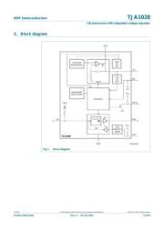
7. Functional description
The TJA1028 combines the functionality of a LIN transceiver and a voltage regulator in a
single chip and offers wake-up by bus activity. The voltage regulator is designed to power
the Electronic Control Unit’s (ECU) microcontroller and its peripherals.
The LIN transceiver is the interface between a LIN master/slave protocol controller and
the physical bus in a LIN network. According to the Open System Interconnect (OSI)
model, these modules make up the LIN physical layer.
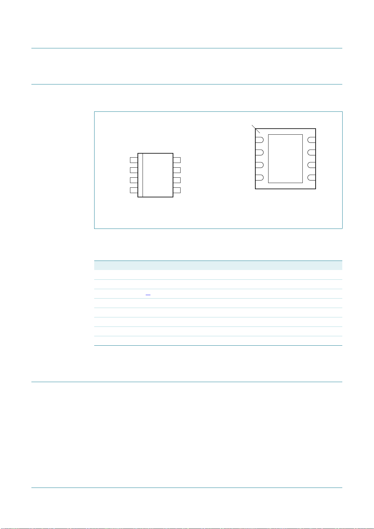
a. TJA1028T/xxx/xx: SO8 b. TJA1028TK/xxx/xx: HVSON8
Fig 2. Pin configuration diagrams
TJA1028T
V
BAT
V
CC
EN
GND
TXD
LIN RXD
015aaa082
1
2
3
4
6
5
8
7
RSTN
015aaa244
TJA1028TK
RXD
GND
LIN
TXD
EN RSTN
V
BAT
V
CC
Transparent top view
4
5
3 6
2 7
1 8
terminal 1
index area
Table 3. Pin description
Symbol Pin Description
V
BAT
1 battery supply for the TJA1028
EN 2 enable input
GND 3
[1]
ground
LIN 4 LIN bus line
RXD 5 LIN receive data output
TXD 6 LIN transmit data input
RSTN 7 reset output (active LOW)
V
CC
8 voltage regulator output
器件 Datasheet 文档搜索
AiEMA 数据库涵盖高达 72,405,303 个元件的数据手册,每天更新 5,000 多个 PDF 文件
