Datasheet 搜索 > 稳压芯片 > TI(德州仪器) > TL1963AKTTR 数据手册 > TL1963AKTTR 数据手册 4/39 页

¥ 7.242
TL1963AKTTR 数据手册 - TI(德州仪器)
制造商:
TI(德州仪器)
分类:
稳压芯片
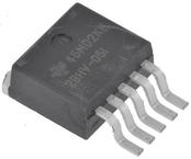
封装:
TO-263-6
描述:
TEXAS INSTRUMENTS TL1963AKTTR. 电压稳压器, LDO, 可调, 2.1V至20V输入, 340mV压差, 1.21V至20V/1.5A输出, TO-263-5
Pictures:
3D模型
符号图
焊盘图
引脚图
产品图
页面导航:
引脚图在P3P4Hot
典型应用电路图在P16P17
原理图在P1P13
封装尺寸在P27P28P30P31P32
标记信息在P27P28P29
封装信息在P26P27P28P29P30P31P32
技术参数、封装参数在P5P17
应用领域在P1P16P17P39
电气规格在P5P6P7
导航目录
TL1963AKTTR数据手册
Page:
of 39 Go
若手册格式错乱,请下载阅览PDF原文件
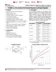
TL1963A
,
TL1963A-15
,
TL1963A-18
,
TL1963A-25
,
TL1963A-33
SLVS719G –JUNE 2008–REVISED JANUARY 2015
www.ti.com
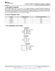
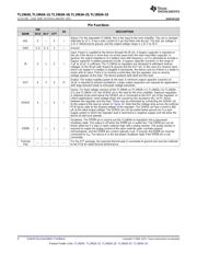
Pin Functions
PIN
I/O DESCRIPTION
NAME DCQ DCY KTT
Adjust. For the adjustable TL1963A, this is the input to the error amplifier. This pin is clamped
ADJ 5 — 5 I internally to ±7 V. It has a bias current of 3 μA that flows into the pin. The ADJ pin voltage is
1.21 V referenced to ground, and the output voltage range is 1.21 V to 20 V.
GND 3, 6 2, 4 3 — Ground
Input. Power is supplied to the device through the IN pin. A bypass capacitor is required on
this pin if the device is more than six inches away from the main input filter capacitor. In
general, the output impedance of a battery rises with frequency, so it is advisable to include a
bypass capacitor in battery-powered circuits. A bypass capacitor (ceramic) in the range of
IN 2 1 2 I 1 μF to 10 μF is sufficient. The TL1963A-xx regulators are designed to withstand reverse
voltages on the IN pin with respect to ground and the OUT pin. In the case of a reverse input,
which can happen if a battery is plugged in backwards, the device acts as if there is a diode in
series with its input. There is no reverse-current flow into the regulator, and no reverse
voltage appears at the load. The device protects both itself and the load.
Output. The output supplies power to the load. A minimum output capacitor (ceramic) of
OUT 4 3 4 O 10 μF is required to prevent oscillations. Larger output capacitors are required for applications
with large transient loads to limit peak voltage transients.
Sense. For fixed voltage versions of the TL1963A-xx (TL1963A-1.5, TL1963A-1.8, TL1963A-
2.5, and TL1963A-3.3), the SENSE pin is the input to the error amplifier. Optimum regulation
is obtained at the point where the SENSE pin is connected to the OUT pin of the regulator. In
critical applications, small voltage drops are caused by the resistance (R
P
) of PC traces
between the regulator and the load. These may be eliminated by connecting the SENSE pin
SENSE 5 — 5 I
to the output at the load as shown in Figure 32. Note that the voltage drop across the external
PCB traces adds to the dropout voltage of the regulator. The SENSE pin bias current is 600
μA at the rated output voltage. The SENSE pin can be pulled below ground (as in a dual
supply system in which the regulator load is returned to a negative supply) and still allow the
device to start and operate.
Shutdown. The SHDN pin is used to put the TL1963A-xx regulators into a low-power
shutdown state. The output is off when the SHDN pin is pulled low. The SHDN pin can be
driven either by 5-V logic or open-collector logic with a pullup resistor. The pullup resistor is
SHDN 1 — 1 I required to supply the pullup current of the open-collector gate, normally several
microamperes, and the SHDN pin current, typically 3 μA. If unused, the SHDN pin must be
connected to V
IN
. The device is in the low-power shutdown state if the SHDN pin is not
connected.
Thermal For the KTT package, the exposed thermal pad is connected to ground and must be soldered
— — — —
Pad to the PCB for rated thermal performance.
4 Submit Documentation Feedback Copyright © 2008–2015, Texas Instruments Incorporated
Product Folder Links: TL1963A TL1963A-15 TL1963A-18 TL1963A-25 TL1963A-33
器件 Datasheet 文档搜索
AiEMA 数据库涵盖高达 72,405,303 个元件的数据手册,每天更新 5,000 多个 PDF 文件
