Datasheet 搜索 > 电压基准芯片 > ON Semiconductor(安森美) > TL431CDR2 数据手册 > TL431CDR2 数据手册 3/20 页
 器件3D模型
¥ 1.667
TL431CDR2 数据手册 - ON Semiconductor(安森美)
制造商:
ON Semiconductor(安森美)
分类:
电压基准芯片
封装:
SOIC-8
描述:
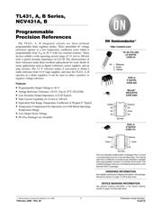
可编程精密基准 PROGRAMMABLE PRECISION REFERENCES
Pictures:
3D模型
符号图
焊盘图
引脚图
产品图
页面导航:
典型应用电路图在P7
原理图在P2
封装尺寸在P17P18P19P20
焊盘布局在P19P20
型号编码规则在P1P13P14P15P16P20
标记信息在P1P16
封装信息在P13P14P15P16
技术参数、封装参数在P13P14P15P16
应用领域在P7P11
电气规格在P3P4
导航目录
TL431CDR2数据手册
Page:
of 20 Go
若手册格式错乱,请下载阅览PDF原文件
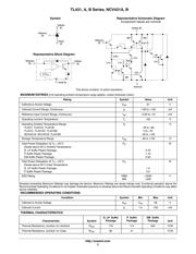
TL431, A, B Series, NCV431A, B
http://onsemi.com
3
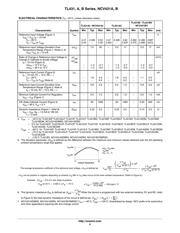
ELECTRICAL CHARACTERISTICS (T
A
= 25°C, unless otherwise noted.)
Characteristic
Symbol
TL431I TL431C
Unit
Min Typ Max Min Typ Max
Reference Input Voltage (Figure 1)
V
KA
= V
ref
, I
K
= 10 mA
T
A
= 25°C
T
A
= T
low
to T
high
(Note 1)
V
ref
2.44
2.41
2.495
-
2.55
2.58
2.44
2.423
2.495
-
2.55
2.567
V
Reference Input Voltage Deviation Over
Temperature Range (Figure 1, Notes 1, 2)
V
KA
= V
ref,
I
K
= 10 mA
DV
ref
- 7.0 30 - 3.0 17 mV
Ratio of Change in Reference Input Voltage to Change
in Cathode to Anode Voltage
I
K
= 10 mA (Figure 2),
DV
KA
= 10 V to V
ref
DV
KA
= 36 V to 10 V
DV
ref
DV
KA
-
-
-1.4
-1.0
-2.7
-2.0
-
-
-1.4
-1.0
-2.7
-2.0
mV/V
Reference Input Current (Figure 2)
I
K
= 10 mA, R1 = 10 k, R2 = ∞
T
A
= 25°C
T
A
= T
low
to T
high
(Note 1)
I
ref
-
-
1.8
-
4.0
6.5
-
-
1.8
-
4.0
5.2
mA
Reference Input Current Deviation Over
Temperature Range (Figure 2, Note 1, 4)
I
K
= 10 mA, R1 = 10 k, R2 = ∞
DI
ref
- 0.8 2.5 - 0.4 1.2
mA
Minimum Cathode Current For Regulation
V
KA
= V
ref
(Figure 1)
I
min
- 0.5 1.0 - 0.5 1.0 mA
Off-State Cathode Current (Figure 3)
V
KA
= 36 V, V
ref
= 0 V
I
off
- 20 1000 - 20 1000 nA
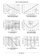
Dynamic Impedance (Figure 1, Note 3)
V
KA
= V
ref
, DI
K
= 1.0 mA to 100 mA
f ≤ 1.0 kHz
|Z
KA
| - 0.22 0.5 - 0.22 0.5
W
1. T
low
= -40°C for TL431AIP TL431AILP, TL431IP, TL431ILP, TL431BID, TL431BIP, TL431BILP, TL431AIDM, TL431IDM, TL431BIDM;
=0°C for TL431ACP, TL431ACLP, TL431CP, TL431CLP, TL431CD, TL431ACD, TL431BCD, TL431BCP, TL431BCLP, TL431CDM,
TL431ACDM, TL431BCDM
T
high
= +85°C for TL431AIP, TL431AILP, TL431IP, TL431ILP, TL431BID, TL431BIP, TL431BILP, TL431IDM, TL431AIDM, TL431BIDM
= +70°C for TL431ACP, TL431ACLP, TL431CP, TL431ACD, TL431BCD, TL431BCP, TL431BCLP, TL431CDM, TL431ACDM,
TL431BCDM
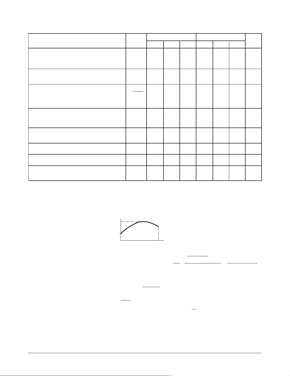
2. The deviation parameter DV
ref
is defined as the difference between the maximum and minimum values obtained over the full operating
ambient temperature range that applies.
DV
ref
= V
ref
max
-V
ref
min
DT
A
= T
2
- T
1
T2
Ambient Temperature
T1
V
ref
min
V
ref
max
The average temperature coefficient of the reference input voltage, aV
ref
is defined as:
V
ref
ppm
_C
+
ǒ
DV
ref
V
ref
@25_C
Ǔ
X10
6
DT
A
+
DV
ref
x10
6
DT
A
(V
ref
@25_C)
aV
ref
can be positive or negative depending on whether V
ref
Min or V
ref
Max occurs at the lower ambient temperature. (Refer to Figure 6.)
Example : DV
ref
+ 8.0mV and slopeispositive,
V
ref
@25_C + 2.495V, DT
A
+ 70_C
aV
ref
+
0.008x10
6
70(2.495)
+ 45.8ppmń_C
3. The dynamic impedance Z
KA
is defined as:
|Z
KA
| +
DV
KA
DI
K
. When the device is programmed with two external resistors, R1 and R2,
(refer to Figure 2) the total dynamic impedance of the circuit is defined as:
|Z
KA
Ȁ| [ |Z
KA
|
ǒ
1 )
R1
R2
Ǔ
器件 Datasheet 文档搜索
AiEMA 数据库涵盖高达 72,405,303 个元件的数据手册,每天更新 5,000 多个 PDF 文件
