Datasheet 搜索 > AD转换器 > TI(德州仪器) > TLC549IPSR 数据手册 > TLC549IPSR 数据手册 5/19 页
 器件3D模型
¥ 12.012
TLC549IPSR 数据手册 - TI(德州仪器)
制造商:
TI(德州仪器)
分类:
AD转换器
封装:
SOP-8
描述:
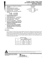
8位模拟数字转换器带串行控制 8-BIT ANALOG-TO-DIGITAL CONVERTERS WITH SERIAL CONTROL
Pictures:
3D模型
符号图
焊盘图
引脚图
产品图
页面导航:
封装尺寸在P10P11P13P14
标记信息在P10P11
封装信息在P10P11P12P13P14
应用领域在P1P7
导航目录
TLC549IPSR数据手册
Page:
of 19 Go
若手册格式错乱,请下载阅览PDF原文件
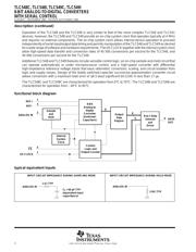
TLC548C, TLC548I, TLC549C, TLC549I
8-BIT ANALOG-TO-DIGITAL CONVERTERS
WITH SERIAL CONTROL
SLAS067C – NOVEMBER 1983 – REVISED SEPTEMBER 1996
5
POST OFFICE BOX 655303 • DALLAS, TEXAS 75265
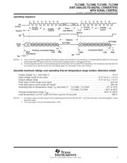
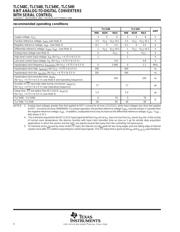
electrical characteristics over recommended operating free-air temperature range,
V
CC
= V
ref+
= 4.75 V to 5.5 V, f
clock(I/O)
= 2.048 MHz for TLC548 or 1.1 MHz for TLC549
(unless otherwise noted)
PARAMETER TEST CONDITIONS MIN TYP
†
MAX UNIT
V
OH
High-level output voltage V
CC
= 4.75 V, I
OH
= –360 µA 2.4 V
V
OL
Low-level output voltage V
CC
= 4.75 V, I
OL
= 3.2 mA 0.4 V
I
OZ
High im
p
edance off state out
p
ut current
V
O
= V
CC
, CS at V
CC
10
µA
I
OZ
High
-
impedance
off
-
state
o
u
tp
u
t
c
u
rrent
V
O
= 0, CS at V
CC
–10
µ
A
I
IH
High-level input current, control inputs V
I
= V
CC
0.005 2.5 µA
I
IL
Low-level input current, control inputs V
I
= 0 –0.005 –2.5 µA
I
I( )
Analog channel on-state input current during sample
Analog input at V
CC
0.4 1
µA
I
I(on)
gg
cycle
Analog input at 0 V
–0.4 –1
µ
A
I
CC
Operating supply current CS at 0 V 1.8 2.5 mA
I
CC
+ I
ref
Supply and reference current V
ref+
= V
CC
1.9 3 mA
C
i
In
p
ut ca
p
acitance
Analog inputs 7 55
p
F
C
i
Inp
u
t
capacitance
Control inputs 5 15
pF
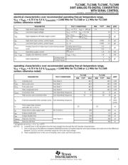
operating characteristics over recommended operating free-air temperature range,
V
CC
= V
ref+
= 4.75 V to 5.5 V, f
clock(I/O)
= 2.048 MHz for TLC548 or 1.1 MHz for TLC549
(unless otherwise noted)
PARAMETER
TEST CONDITIONS
TLC548 TLC549
UNIT
PARAMETER
TEST
CONDITIONS
MIN
TYP
†
MAX MIN TYP
†
MAX
UNIT
E
L
Linearity error See Note 6 ±0.5 ±0.5 LSB
E
ZS
Zero-scale error See Note 7 ±0.5 ±0.5 LSB
E
FS
Full-scale error See Note 7 ±0.5 ±0.5 LSB
Total unadjusted error See Note 8 ±0.5 ±0.5 LSB
t
conv
Conversion time See Operating Sequence 8 17 12 17 µs
Total access and conversion time See Operating Sequence 12 22 19 25 µs
t
a
Channel acquisition time (sample cycle) See Operating Sequence 4 4
I/O
clock
cycles
t
v
Time output data remains
valid after I/O CLOCK↓
10 10 ns
t
d
Delay time to data output valid I/O CLOCK↓ 200 400 ns
t
en
Output enable time 1.4 1.4 µs
t
dis
Output disable time 150 150 ns
t
r(bus)
Data bus rise time
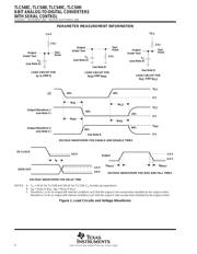
See Figure 1
300 300 ns
t
f(bus)
Data bus fall time 300 300 ns
†
All typicals are at V
CC
= 5 V, T
A
= 25°C.
NOTES: 6. Linearity error is the deviation from the best straight line through the A/D transfer characteristics.
7. Zero-scale error is the difference between 00000000 and the converted output for zero input voltage; full-scale error is the difference
between 11111111 and the converted output for full-scale input voltage.
8. Total unadjusted error is the sum of linearity, zero-scale, and full-scale errors.
器件 Datasheet 文档搜索
AiEMA 数据库涵盖高达 72,405,303 个元件的数据手册,每天更新 5,000 多个 PDF 文件
