Datasheet 搜索 > LED驱动器 > TI(德州仪器) > TLC59116IPWR 数据手册 > TLC59116IPWR 数据手册 6/39 页
 器件3D模型
¥ 4.387
TLC59116IPWR 数据手册 - TI(德州仪器)
制造商:
TI(德州仪器)
分类:
LED驱动器
封装:
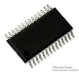
TSSOP-28
描述:
TEXAS INSTRUMENTS TLC59116IPWR 芯片, 发光二极管驱动器, 恒流, TSSOP28, 整卷
Pictures:
3D模型
符号图
焊盘图
引脚图
产品图
页面导航:
典型应用电路图在P13
原理图在P2
封装尺寸在P2P29P31P32
型号编码规则在P1P2
标记信息在P2P29
封装信息在P2P29P30P31P32
功能描述在P10
技术参数、封装参数在P5
应用领域在P39
电气规格在P6
导航目录
TLC59116IPWR数据手册
Page:
of 39 Go
若手册格式错乱,请下载阅览PDF原文件
TLC59116
SLDS157D –FEBRUARY 2008– REVISED JULY 2011
www.ti.com
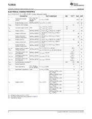
ELECTRICAL CHARACTERISTICS
V
CC
= 3 V to 5.5 V, T
A
= –40°C to 85°C (unless otherwise noted)
PARAMETER TEST CONDITIONS MIN TYP
(1)
MAX UNIT
SCL, SDA, A0,
Input/output leakage
I
I
A1, A2, A3, V
I
= V
CC
or GND ±0.3 μA
current
RESET
Output leakage current OUT0 to OUT15 V
O
= 17 V, T
J
= 25°C 0.5 μA
V
POR
Power-on reset voltage 2.5 V
V
CC
= 3 V, V
OL
= 0.4 V 20
I
OL
Low-level output current SDA mA
V
CC
= 5 V, V
OL
= 0.4 V 30
I
O(1)
Output current 1 OUT0 to OUT15 V
O
= 0.6 V, R
ext
= 720 Ω, CG = 0.992
(2)
26 mA
I
O
= 26 mA, V
O
= 0.6 V, R
ext
= 720 Ω,
Output current error OUT0 to OUT15 ±8 %
T
J
= 25°C
Output channel to I
O
= 26 mA, V
O
= 0.6 V, R
ext
= 720 Ω,
OUT0 to OUT15 ±6 %
channel current error T
J
= 25°C
I
O(2)
Output current 2 OUT0 to OUT15 V
O
= 0.8 V, R
ext
= 360 Ω, CG = 0.992
(2)
52 mA
I
O
= 52 mA, V
O
= 0.8 V, R
ext
= 360 Ω,
Output current error OUT0 to OUT15 ±8 %
T
J
= 25°C
Output channel to I
O
= 52 mA, V
O
= 0.8 V, R
ext
= 360 Ω,
OUT0 to OUT15 ±6 %
channel current error T
J
= 25°C
V
O
= 1 V to 3 V, I
O
= 26 mA ±0.1
I
OUT
vs Output current vs output
OUT0 to OUT15 %/V
V
OUT
voltage regulation
V
O
= 3 V to 5.5 V, I
O
= 26 mA to 120 mA ±1
Threshold current 1 for 0.5 ×
I
OUT,Th1
OUT0 to OUT15 I
OUT,target
= 26 mA %
error detection I
TARGET
Threshold current 2 for 0.5 ×
I
OUT,Th2
OUT0 to OUT15 I
OUT,target
= 52 mA %
error detection I
TARGET
Threshold current 3 for 0.5 ×
I
OUT,Th3
OUT0 to OUT15 I
OUT,target
= 104 mA %
error detection I
TARGET
T
SD
Overtemperature shutdown
(3)
150 175 200 °C
T
HYS
Restart hysteresis 15 °C
SCL, A0, A1,
C
i
Input capacitance V
I
= V
CC
or GND 5 pF
A2, A3, RESET
C
io
Input/output capacitance SDA V
I
= V
CC
or GND 8 pF
OUT0 to OUT15 = OFF,
25
R
ext
= Open
OUT0 to OUT15 = OFF,
29
R
ext
= 720 Ω
OUT0 to OUT15 = OFF,
32
R
ext
= 360 Ω
OUT0 to OUT15 = OFF,
I
CC
Supply current V
CC
= 5.5 V 37 mA
R
ext
= 180 Ω
OUT0 to OUT15 = ON,
29
R
ext
= 720 Ω
OUT0 to OUT15 = ON,
32
R
ext
= 360 Ω
OUT0 to OUT15 = ON,
37
R
ext
= 180 Ω
(1) All typical values are at T
A
= 25°C.
(2) CG is the Current Gain and is defined in Table 12.
(3) Specified by design
6 Copyright © 2008–2011, Texas Instruments Incorporated
器件 Datasheet 文档搜索
AiEMA 数据库涵盖高达 72,405,303 个元件的数据手册,每天更新 5,000 多个 PDF 文件
