Datasheet 搜索 > 二极管 > Toshiba(东芝) > TLP281 数据手册 > TLP281 数据手册 3/8 页
 器件3D模型
¥ 1.46
TLP281 数据手册 - Toshiba(东芝)
制造商:
Toshiba(东芝)
分类:
二极管
封装:
SOP-4
描述:
TLP281 SOP4 marking/标记 P281
Pictures:
3D模型
符号图
焊盘图
引脚图
产品图
页面导航:
导航目录
TLP281数据手册
Page:
of 8 Go
若手册格式错乱,请下载阅览PDF原文件
TLP281,TLP281-4
2010-08-27 3
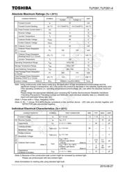
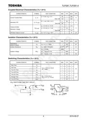
Absolute Maximum Ratings
(Ta = 25°C)
RATING
CHARACTERISTIC SYMBOL
TLP281 TLP281−4
UNIT
Forward Current I
F
50 mA
Forward Current Derating ∆I
F
/°C −0.7 (Ta≥53°C) −0.5 (Ta≥25°C) mA /°C
Pulse Forward Current (Note 1) I
FP
1 A
Reverse Voltage V
R
5 V
LED
Junction Temperature T
j
125 °C
Collector-Emitter Voltage V
CEO
80 V
Emitter-Collector Voltage V
ECO
7 V
Collector Current I
C
50 mA
Collector Power Dissipation
(1 Circuit)
P
C
150 100 mW
Collector Power Dissipation
Derating(Ta≥25°C) (1 Circuit)
∆P
C
/°C −1.5 −1.0 mW /°C
DETECTOR
Junction Temperature T
j
125 °C
Operating Temperature Range T
opr
−55 to 100 °C
Storage Temperature Range T
stg
−55 to 125 °C
Lead Soldering Temperature T
sol
260 (10s) °C
Total Package Power Dissipation
(1 Circuit)
P
T
200 170 mW
Total Package Power Dissipation
Derating (Ta≥25°C) (1 Circuit)
∆P
T
/°C −2.0 −1.7 mW /°C
Isolation Voltage (Note 2) BV
S
2500(AC,1min,R.H.≤60%)
Vrms
Note: Using continuously under heavy loads (e.g. the application of high temperature/current/voltage and the
significant change in temperature, etc.) may cause this product to decrease in the reliability significantly even
if the operating conditions (i.e. operating temperature/current/voltage, etc.) are within the absolute maximum
ratings.
Please design the appropriate reliability upon reviewing the Toshiba Semiconductor Reliability Handbook
(“Handling Precautions”/“Derating Concept and Methods”) and individual reliability data (i.e. reliability test
report and estimated failure rate, etc).
(Note 1) Pulse width ≤ 100μs, frequency 100Hz
(Note 2) AC, 1 minute, R.H.≤60%,Device considered a two terminal device : LED side pins shorted together and
DETECTOR side pins shorted together.
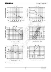
Individual Electrical Characteristics
(Ta = 25°C)
CHARACTERISTIC SYMBOL TEST CONDITION MIN. TYP. MAX. UNIT
Forward Voltage V
F
I
F
= 10 mA 1.0 1.15 1.3 V
Reverse Current I
R
V
R
= 5 V
—
— 10 μA
LED
Capacitance C
T
V = 0, f = 1 MHz
—
30 — pF
Collector-Emitter
Breakdown Voltage
V
(BR) CEO
I
C
= 0.5 mA 80
— —
V
Emitter-Collector
Breakdown Voltage
V
(BR) ECO
I
E
= 0.1 mA 7
— —
V
V
CE
= 48 V,
Ambient Light Below
(100 ℓx) (Note 4)
—
0.01
(2)
0.1
(10)
μA
Collector Dark Current
(Note 3)
I
CEO
V
CE
= 48 V, Ta = 85°C
Ambient Light Below
(100 ℓx) (Note 4)
—
2
(4)
50
(50)
μA
DETECTOR
Capacitance
(Collector to Emitter)
C
CE
V = 0, f = 1 MHz
—
10 — pF
(Note 3) Because of the construction,leak current might be increased by ambient light.
Please use photocoupler with less ambient light.
(Note 4)Irradiation to marking side using standard light bulb.
器件 Datasheet 文档搜索
AiEMA 数据库涵盖高达 72,405,303 个元件的数据手册,每天更新 5,000 多个 PDF 文件
