Datasheet 搜索 > 稳压芯片 > TI(德州仪器) > TLV73333PQDRVRQ1 数据手册 > TLV73333PQDRVRQ1 数据手册 1/27 页
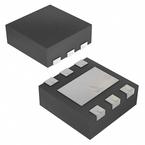
 器件3D模型
¥ 4.519
TLV73333PQDRVRQ1 数据手册 - TI(德州仪器)
制造商:
TI(德州仪器)
分类:
稳压芯片
封装:
WDFN-6
描述:
具有使能功能的汽车类 300mA、低 IQ、低压降稳压器 6-WSON -40 to 150
Pictures:
3D模型
符号图
焊盘图
引脚图
产品图
页面导航:
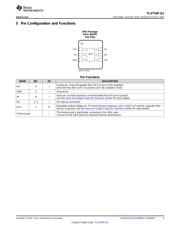
引脚图在P3Hot
典型应用电路图在P1P15
原理图在P10
封装尺寸在P20P22P23
标记信息在P20P21
封装信息在P18P19P20P21P22P23
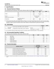
技术参数、封装参数在P4
应用领域在P1P15
电气规格在P5
导航目录
TLV73333PQDRVRQ1数据手册
Page:
of 27 Go
若手册格式错乱,请下载阅览PDF原文件
I
OUT
(mA)
V
DO
(mV)
0 30 60 90 120 150 180 210 240 270 300
0
20
40
60
80
100
120
140
160
180
D020
V
OUT
= 3.3 V
V
OUT
= 1.8 V
TLV733P-Q1
IN
EN
OUT
GND
C
OUT
C
IN
Optional
Optional
ON
OFF
Copyright © 2016, Texas Instruments Incorporated
Product
Folder
Sample &
Buy
Technical
Documents
Tools &
Software
Support &
Community
An IMPORTANT NOTICE at the end of this data sheet addresses availability, warranty, changes, use in safety-critical applications,
intellectual property matters and other important disclaimers. PRODUCTION DATA.
TLV733P-Q1
SBVS283A –AUGUST 2016–REVISED AUGUST 2016
TLV733P-Q1
Capacitor-Free, 300-mA, Low Dropout (LDO) Linear Regulator
1
1 Features
1
• Qualified for Automotive Applications
• AEC-Q100 Qualified:
– Device Temperature Grade 1: –40°C to 125°C
Ambient Operating Temperature
– Device HBM ESD Classification Level 2
– Device CDM ESD Classification Level C4B
• Input Voltage Range: 1.4 V to 5.5 V
• Stable Operation With or Without Capacitors
• Foldback Overcurrent Protection
• Package:
– 2.0-mm × 2.0-mm WSON-6
• Very Low Dropout: 125 mV at 300 mA (3.3 V
OUT
)
• Accuracy: 1% Typical, 1.4% Maximum
• Low I
Q
: 34 µA
• Available in Fixed-Output Voltages:
1.0 V to 3.3 V
• High PSRR: 50 dB at 1 kHz
• Active Output Discharge
2 Applications
• Camera Modules
• Automotive Infotainment
• Navigation Systems
3 Description
The TLV733P-Q1 family of low dropout (LDO) linear
regulators are ultra-small, low quiescent current
LDOs that can source 300 mA with good line and
load transient performance. These devices provide a
typical accuracy of 1%.
The TLV733P-Q1 family is designed with a modern
capacitor-free architecture to ensure stability without
an input or output capacitor. The removal of the
output capacitor allows for a very small solution size,
and can eliminate inrush current at startup.
Furthermore, the TLV733P-Q1 family is also stable
with ceramic output capacitors if an output capacitor
is necessary. The TLV733P-Q1 family also provides
foldback current control during device power-up and
enabling if an output capacitor is used. This
functionality is especially important in battery-
operated devices.
The TLV733P-Q1 family provides an active pulldown
circuit to quickly discharge output loads when
disabled.
The TLV733P-Q1 family is available in the 6-pin DRV
(WSON) package.
Device Information
(1)
PART NUMBER PACKAGE BODY SIZE (NOM)
TLV733P-Q1 WSON (6) 2.00 mm × 2.00 mm
(1) For all available packages, see the package option addendum
at the end of the data sheet.
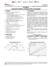
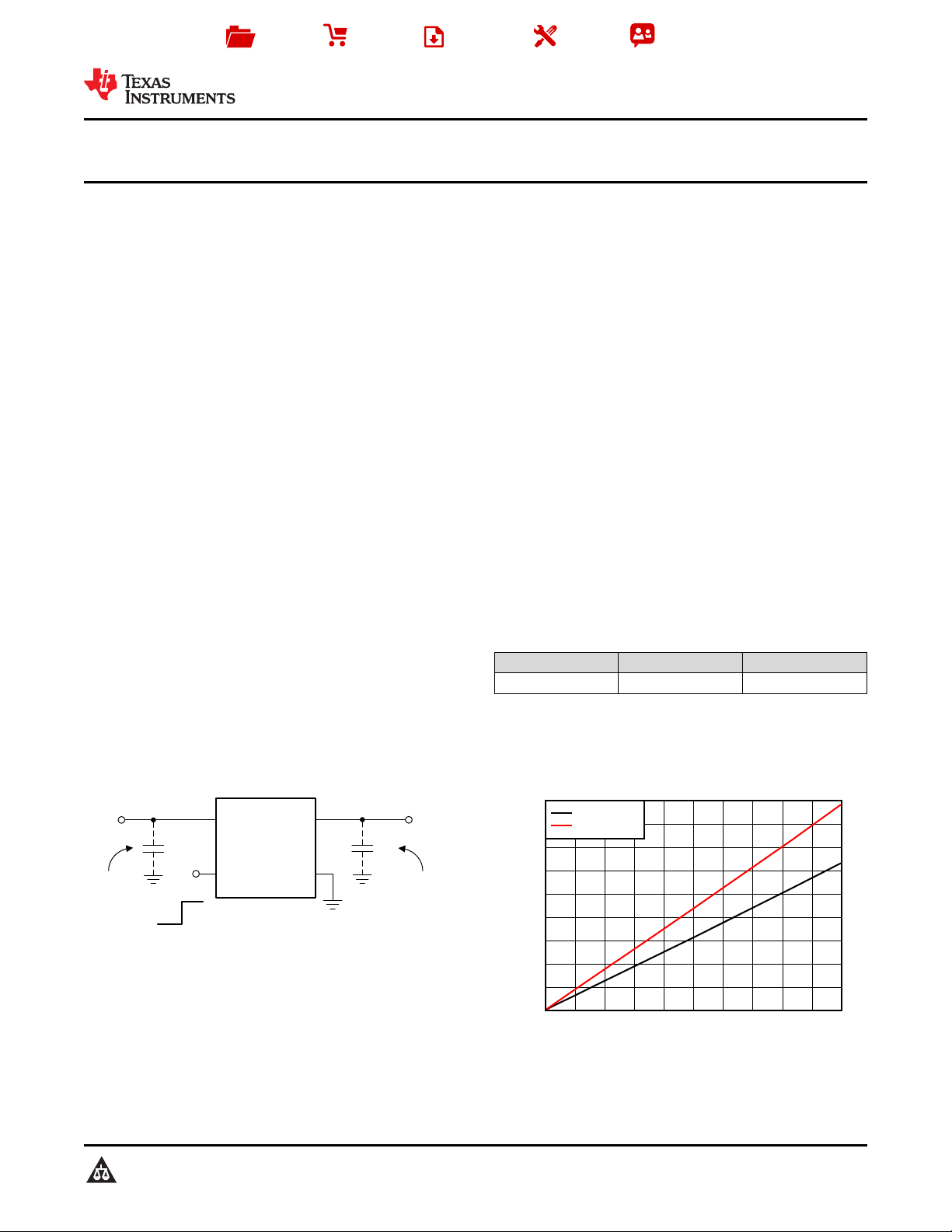
Typical Application Circuit Dropout Voltage vs Output Current
器件 Datasheet 文档搜索
AiEMA 数据库涵盖高达 72,405,303 个元件的数据手册,每天更新 5,000 多个 PDF 文件
