Datasheet 搜索 > DSP数字信号处理器 > TI(德州仪器) > TMS320C5515AZCH12 数据手册 > TMS320C5515AZCH12 数据手册 65/160 页
 器件3D模型
¥ 75.135
TMS320C5515AZCH12 数据手册 - TI(德州仪器)
制造商:
TI(德州仪器)
分类:
DSP数字信号处理器
封装:
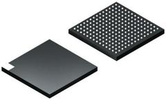
NFBGA-196
描述:
DSP),Texas Instruments德州仪器数字信号处理器是微处理器,带有一个优化的体系结构,用于数字信号处理的运算需求。### 数字信号处理器,Texas Instruments
Pictures:
3D模型
符号图
焊盘图
引脚图
产品图
页面导航:
引脚图在P15P62P65Hot
典型应用电路图在P138
原理图在P4
封装尺寸在P157
封装信息在P156P157P158
功能描述在P61
技术参数、封装参数在P12P71P76P77P78P79P80P81P82P83P84P85
应用领域在P1P160
电气规格在P12P38P42P69P73P74P75P76P77P78P79P80
导航目录
TMS320C5515AZCH12数据手册
Page:
of 160 Go
若手册格式错乱,请下载阅览PDF原文件

TMS320C5515
www.ti.com
SPRS645C–AUGUST 2010– REVISED MARCH 2011
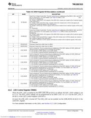
4.6.6 Output Slew Rate Control Register (OSRCR) [1C16h]
To provide the lowest power consumption setting, the DSP has configurable slew rate control on the EMIF
and CLKOUT output pins. The output slew rate control register (OSRCR) is used to set a subset of the
device I/O pins, namely CLKOUT and EMIF pins, to either fast or slow slew rate. The slew rate feature is
implemented by staging/delaying turn-on times of the parallel p-channel drive transistors and parallel
n-channel drive transistors of the output buffer. In the slow slew rate configuration, the delay is longer, but
ultimately the same number of parallel transistors are used to drive the output high or low. Thus, the drive
strength is ultimately the same. The slower slew rate control can be used for power savings and has the
greatest effect at lower DV
DDIO
and DV
DDEMIF
voltages.
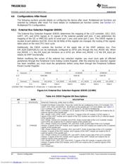
4.7 Multiplexed Pin Configurations
The device DSP uses pin multiplexing to accommodate a larger number of peripheral functions in the
smallest possible package, providing the ultimate flexibility for end applications. The external bus selection
register (EBSR) controls all the pin multiplexing functions on the device.
4.7.1 Pin Multiplexing Details
This section discusses how to program the external bus selection register (EBSR) to select the desired
peripheral functions and pin muxing. See the individual pin mux sections for pin muxing details for a
specific muxed pin. After changing any of the pin mux control registers, it will be necessary to reset the
peripherals that are affected.
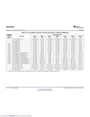
4.7.1.1 LCD Controller, SPI, UART, I2S2, I2S3, and GP[31:27, 20:18] Pin Multiplexing [EBSR.PPMODE
Bits]
The LCD Controller, SPI, UART, I2S2, I2S3, and GPIO signal muxing is determined by the value of the
PPMODE bit fields in the External Bus Selection Register (EBSR) register. For more details on the actual
pin functions, see Table 4-7.
Copyright © 2010–2011, Texas Instruments Incorporated Device Configuration 65
Submit Documentation Feedback
Product Folder Link(s): TMS320C5515
Downloaded from Elcodis.com electronic components distributor
器件 Datasheet 文档搜索
AiEMA 数据库涵盖高达 72,405,303 个元件的数据手册,每天更新 5,000 多个 PDF 文件
