Datasheet 搜索 > DSP数字信号处理器 > TI(德州仪器) > TMS320C6421ZDUQ5 数据手册 > TMS320C6421ZDUQ5 数据手册 92/222 页
 器件3D模型
¥ 46.15
TMS320C6421ZDUQ5 数据手册 - TI(德州仪器)
制造商:
TI(德州仪器)
分类:
DSP数字信号处理器
封装:
BGA-376
描述:
数字信号处理器和控制器 - DSP, DSC Fixed-Pt Dig Signal Proc
Pictures:
3D模型
符号图
焊盘图
引脚图
产品图
页面导航:
引脚图在P16P29P33P74P75P77P79P84P85P86P90P91Hot
原理图在P4P107P108P117P118P166P184
封装尺寸在P218P219
标记信息在P218P219
封装信息在P217P218P219
技术参数、封装参数在P109P113P114P115P116P117P118P119P120P121P122P123
应用领域在P2P110P222
电气规格在P106P111P112P113P114P115P116P117P118P119P120P121

导航目录
TMS320C6421ZDUQ5数据手册
Page:
of 222 Go
若手册格式错乱,请下载阅览PDF原文件
3.7.3.5 UART0 Flow Control Block
3.7.3.6 Timer0 Block
TMS320C6421
Fixed-Point Digital Signal Processor
SPRS346D – JANUARY 2007 – REVISED JUNE 2008
www.ti.com
In addition, the VDD3P3V_PWDN.UR0DAT field determines the power state of the UART0 Data Block
pins. The UART0 Data Block pins default to powered down and not operational. To use these pins, user
must first program VDD3P3V_PWDN.UR0DAT = 0 to power up the pins. For more details on the
VDD3P3V_PWDN.UR0DAT field, see Section 3.2 , Power Considerations.
The UART0 Data Block features internal pullup resistors, which matches the UART inactive polarity.
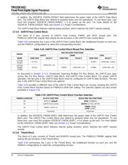
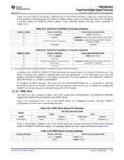
This block of 2 pins consists of UART0 Flow Control, PWM0, and GPIO muxed pins. The
PINMUX1.UR0FCBK register field selects the pin functions in the UART0 Flow Control Block.
Table 3-24 summarizes the 2 pins in the UART0 Flow Control Block, the multiplexed function on each pin,
and the PINMUX configurations to select the corresponding function.
Table 3-24. UART0 Flow Control Block Muxed Pins Selection
MULTIPLEXED FUNCTIONS
SIGNAL
UART0 PWM0 GPIO
NAME FUNCTION SELECT FUNCTION SELECT FUNCTION SELECT
UCTS0/
UCTS0 – – GP[87] UR0FCBK = 00/10
GP[87]
UR0FCBK = 01
URTS0/
PWM0/ URTS0 PWM0 UR0FCBK = 10 GP[88] UR0FCBK = 00
GP[88]
As discussed in Section 3.7.3.2 , Peripherals Spanning Multiple Pin Mux Blocks, the UART0 pins span
across two Pin Mux Blocks: UART0 Data Block, and UART0 Flow Control Block. For proper UART0
operation, the two pins in the UART0 Data Block must be configured for UART0 data functions. The two
pins in the UART0 Flow Control Block are optional.
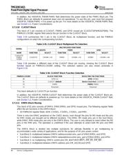
Table 3-25 provides a different view of the UART0 Flow Control Block pin muxing, showing the UART0
Flow Control Block function based on PINMUX1.UR0FCBK setting. The selection options are also shown
pictorially in Figure 3-10 .
Table 3-25. UART0 Flow Control Block Function Selection
PINMUX1.UR0FCBK BLOCK FUNCTION RESULTING PIN FUNCTIONS
00 GPIO (2) ( default) GPIO: GP[88:87]
01 UART0 Flow Control UART0: UCTS0, URTS0
PWM0: PWM0
10 PWM0 + GPIO (1)
GPIO: GP[87]
11 Reserved Reserved
In addition, the VDD3P3V_PWDN.UR0FC field determines the power state of the UART0 Flow Control
Block pins. The UART0 Flow Control Block pins default to powered down and not operational. To use
these pins, user must first program VDD3P3V_PWDN.UR0FC = 0 to power up the pins. For more details
on the VDD3P3V_PWDN.UR0FC field, see Section 3.2 , Power Considerations.
The UART0 Flow Control Block features internal pullup resistors, which matches the UART inactive
polarity.
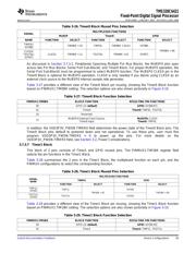
This block of 2 pins consists of Timer0 and McBSP0 muxed pins. The PINMUX1.TIM0BK register field
selects the pin functions in the Timer0 Block.
Table 3-26 summarizes the 2 pins in the Timer0 Block, the multiplexed function on each pin, and the
PINMUX configurations to select the corresponding function.
Device Configurations92 Submit Documentation Feedback
器件 Datasheet 文档搜索
AiEMA 数据库涵盖高达 72,405,303 个元件的数据手册,每天更新 5,000 多个 PDF 文件
