Datasheet 搜索 > DSP数字信号处理器 > TI(德州仪器) > TMS320DM647ZUT7 数据手册 > TMS320DM647ZUT7 数据手册 101/191 页
 器件3D模型
¥ 112.316
TMS320DM647ZUT7 数据手册 - TI(德州仪器)
制造商:
TI(德州仪器)
分类:
DSP数字信号处理器
封装:
FCBGA-529
描述:
数字媒体处理器 Digital Media Processor
Pictures:
3D模型
符号图
焊盘图
引脚图
产品图
页面导航:
引脚图在P16Hot
原理图在P4P101P102P103P130P134P154P163
封装尺寸在P185P186P187P188
标记信息在P185P186P187P188P189
封装信息在P184P185P186P187P188P189
技术参数、封装参数在P54P57P58P59P60P61P62P63P64P65P66P67
应用领域在P2
电气规格在P49P56P57P58P59P60P61P62P63P64P65P66
导航目录
TMS320DM647ZUT7数据手册
Page:
of 191 Go
若手册格式错乱,请下载阅览PDF原文件
TMS320DM647
TMS320DM648
www.ti.com
SPRS372H –MAY 2007–REVISED APRIL 2012
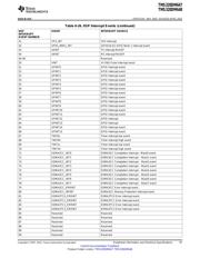
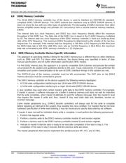
6.9.2 DDR2 Memory Controller Peripheral Registers
Table 6-28. DDR2 Memory Controller Registers
(1)
HEX ADDRESS RANGE ACRONYM REGISTER NAME
0x7800 0000 MIDR DDR2 Memory Controller Module and Revision Register
0x7800 0004 DMCSTAT DDR2 Memory Controller Status Register
0x7800 0008 SDCFG DDR2 Memory Controller SDRAM Configuration Register
0x7800 000C SDRFC DDR2 Memory Controller SDRAM Refresh Control Register
0x7800 0010 SDTIM1 DDR2 Memory Controller SDRAM Timing 1 Register
0x7800 0014 SDTIM2 DDR2 Memory Controller SDRAM Timing 2 Register
0x7800 0018 - Reserved
0x7800 0020 BPRIO DDR2 Memory Controller Burst Priority Register
0x7800 0024 - 0x7800 004C - Reserved
0x7800 0050 - 0x7800 0078 - Reserved
0x7800 007C - 0x7800 00BC - Reserved
0x7800 00C0 - 0x7800 00E0 - Reserved
0x7800 00E4 DMCCTL DDR2 Memory Controller Control Register
0x7800 00E8 - 0x7800 00FC - Reserved
0x7800 0100 - 0x7FFF FFFF - Reserved
(1) For details about the DDR2 registers and their modes, see the TMS320DM647/DM648 DSP DDR2 Memory Controller (DDR2) User's
Guide (literature number SPRUEK5).
6.9.3 DDR2 Interface
This section provides the timing information for the DDR2 interface as a PCB design and manufacturing
specification. The design rules constrain PCB trace length, PCB trace skew, signal integrity, cross-talk,
and signal timing. These rules, when followed, result in a reliable DDR2 memory system without the need
for a complex timing closure process. For more information regarding guidelines for using this DDR2
specification, Understanding TI's PCB Routing Rule-Based DDR2 Timing Specification (SPRAAV0).
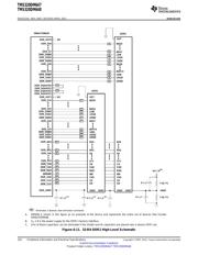
6.9.3.1 DDR2 Interface Schematic
Figure 6-11 shows the DDR2 interface schematic for a x32 DDR2 memory system. The x16 DDR2 system
schematic shown in Figure 6-12 is identical except that the high word DDR2 device is deleted.
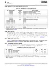
6.9.3.2 Compatible JEDEC DDR2 Devices
Table 6-29 shows the parameters of the JEDEC DDR2 devices that are compatible with this interface.
Generally, the DDR2 interface is compatible with x16 DDR2-533 speed grade DDR2 devices.
Table 6-29. Compatible JEDEC DDR2 Devices
NO. PARAMETER MIN MAX UNIT
1 JEDEC DDR2 Device Speed Grade
(1)
DDR2-533
2 JEDEC DDR2 Device Bit Width x16 x16 Bits
3 JEDEC DDR2 Device Count
(2)
1 2 Devices
4 JEDEC DDR2 Device Ball Count
(3)
84 92 Balls
(1) Higher DDR2 speed grades are supported due to inherent JEDEC DDR2 backwards compatibility.
(2) One DDR2 device is used for 16-bit DDR2 memory system. Two DDR2 devices are used for 32-bit DDR2 memory system.
(3) 92 ball devices retained for legacy support. New designs will migrate to 84 ball DDR2 devices. Electrically, the 92 and 84 ball DDR2
devices are the same.
Copyright © 2007–2012, Texas Instruments Incorporated Peripheral Information and Electrical Specifications 101
Submit Documentation Feedback
Product Folder Link(s): TMS320DM647 TMS320DM648
器件 Datasheet 文档搜索
AiEMA 数据库涵盖高达 72,405,303 个元件的数据手册,每天更新 5,000 多个 PDF 文件
