Datasheet 搜索 > 微控制器 > TI(德州仪器) > TMS320F28032PAGQ 数据手册 > TMS320F28032PAGQ 数据手册 5/160 页
 器件3D模型
¥ 71.106
TMS320F28032PAGQ 数据手册 - TI(德州仪器)
制造商:
TI(德州仪器)
分类:
微控制器
封装:
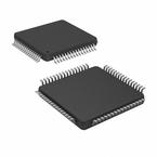
TQFP-64
描述:
Piccolo微处理器 Piccolo Microcontrollers
Pictures:
3D模型
符号图
焊盘图
引脚图
产品图
页面导航:
引脚图在P9P78Hot
典型应用电路图在P48P94
原理图在P3P76P91P96P105P108P110P124P126P129
封装尺寸在P156P157P158
标记信息在P156P157P158P159
封装信息在P2P150P156P157P158P159
技术参数、封装参数在P21P22P23P24P25P26P27P28P29P30P31P32
应用领域在P1P67P123P127P144
电气规格在P27P45P64P83P92
型号编号列表在P110
导航目录
TMS320F28032PAGQ数据手册
Page:
of 160 Go
若手册格式错乱,请下载阅览PDF原文件
5
TMS320F28030
,
TMS320F28031
,
TMS320F28032
TMS320F28033
,
TMS320F28034
,
TMS320F28035
www.ti.com
SPRS584K –APRIL 2009–REVISED JUNE 2016
Submit Documentation Feedback
Product Folder Links: TMS320F28030 TMS320F28031 TMS320F28032 TMS320F28033 TMS320F28034
TMS320F28035
Revision HistoryCopyright © 2009–2016, Texas Instruments Incorporated
2 Revision History
Changes from October 7, 2013 to June 24, 2016 (from J Revision (October 2013) to K Revision) Page
• Global: Changed product status of TMS320F2803x 56-pin RSH devices from TMX (experimental device) to
TMS (fully qualified production device). ........................................................................................... 1
• Global: Restructured document. .................................................................................................. 1
• Global: Added ESD Ratings table; Detailed Description section; Device and Documentation Support section;
and Mechanical Packaging and Orderable Information section. ............................................................... 1
• Global: Removed "Analog MUX" table (this was Table 4-21 in SPRS584J). ............................................... 1
• Global: Removed references to the Reliability Data for TMS320LF24xx and TMS320F28xx Devices Application
Report. ................................................................................................................................. 1
• Global: Replaced "CAN 2.0B" with "ISO11898-1 (CAN 2.0B)". ............................................................... 1
• Section 1.1 (Features): Removed "Dynamic PLL Ratio Changes Supported" feature. ..................................... 1
• Device Information: Added table. .................................................................................................. 2
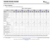
• Table 3-1 (Device Comparison): Changed title from "Hardware Features" to "Device Comparison". .................... 6
• Table 3-1: Removed "Product status" row and associated footnote. ......................................................... 6
• Section 3.1 (Related Products): Added section. ................................................................................. 8
• Section 4.2 (Signal Descriptions): Updated NOTE. ............................................................................ 13
• Table 4-1 (Signal Descriptions): Changed title from "Terminal Functions" to "Signal Descriptions". .................... 13
• Table 4-1: Updated DESCRIPTION of X1, XRS, V
REFHI
, V
REFLO
, V
DD
, and V
DDIO
. ......................................... 13
• Section 5.1 (Absolute Maximum Ratings): Added Input voltage, V
IN
(X1). ................................................. 21
• Section 5.3 (Recommended Operating Conditions): Changed "Junction temperature, T
J
" to "Ambient
temperature, T
A
" for T version and S version. .................................................................................. 22
• Section 5.3: Removed "V
DDIO
and V
DDA
should be maintained within ~0.3 V of each other" footnote. .................. 22
• Section 5.4 (Power Consumption Summary): Changed section title from "Current Consumption" to "Power
Consumption Summary". .......................................................................................................... 23
• Section 5.11 (Power Sequencing): Updated "There is no power sequencing requirement needed ..." paragraph. ... 32
• Table 5-7 (Internal Zero-Pin Oscillator (INTOSC1/INTOSC2) Characteristics): Updated footnote about oscillator
accuracy. ............................................................................................................................ 36
• Figure 6-5 (VREG + POR + BOR + Reset Signal Connectivity): Updated figure. ......................................... 60
• Table 6-13 (PLL, Clocking, Watchdog, and Low-Power Mode Registers): Added PCLKCR2. .......................... 61
• Figure 6-6 (Clock and Reset Domains): Added PCLKCR2. .................................................................. 62
• Section 6.6.2 (Crystal Oscillator Option): Added "The on-chip crystal oscillator X1 and X2 pins are 1.8-V level
signals ..." paragraph. .............................................................................................................. 64
• Figure 6-11 (CPU-watchdog Module): Updated figure. ........................................................................ 68
• Table 6-37 (SPI Master Mode External Timing (Clock Phase = 0)): Parameter 9 [t
v(SPCL-SOMI)M
, t
v(SPCH-SOMI)M
]:
Changed MIN values to 0. ......................................................................................................... 97
• Table 6-38 (SPI Master Mode External Timing (Clock Phase = 1)): Parameter 11 [t
v(SPCH-SOMI)M
, t
v(SPCL-SOMI)M
]:
Changed MIN values to 0. ......................................................................................................... 99
• Table 6-39 (SPI Slave Mode External Timing (Clock Phase = 0)): Parameter 16 [t
v(SPCL-SOMI)S
, t
v(SPCH-SOMI)S
]:
Changed MIN values to 0. ....................................................................................................... 101
• Table 6-40 (SPI Slave Mode External Timing (Clock Phase = 1)): Parameter 18 [t
v(SPCL-SOMI)S
, t
v(SPCH-SOMI)S
]:
Changed MIN values to 0. ....................................................................................................... 102
• Section 6.9.15 (Pin Multiplexing): Changed title from "GPIO MUX" to "General-Purpose Input/Output (GPIO)
MUX". ............................................................................................................................... 132
• Table 6-64 (Analog MUX for 80-Pin PN Package): Added table. .......................................................... 134
• Table 6-65 (Analog MUX for 56-Pin RSH and 64-Pin PAG Packages): Added table. ................................... 135
• Section 7 (Applications, Implementation, and Layout): Added section. .................................................... 144
• Section 8 (Device and Documentation Support): Added section. .......................................................... 145
• Section 8.1 (Getting Started): Updated links. ................................................................................. 145
• Section 8.3 (Tools and Software): Added section. ........................................................................... 146
• Section 8.4 (Documentation Support): Updated section. .................................................................... 147
• Section 9.1 (Packaging Information): Updated section. ...................................................................... 150
器件 Datasheet 文档搜索
AiEMA 数据库涵盖高达 72,405,303 个元件的数据手册,每天更新 5,000 多个 PDF 文件
