Datasheet 搜索 > 微控制器 > TI(德州仪器) > TMS320F28032PAGQ 数据手册 > TMS320F28032PAGQ 数据手册 94/160 页
 器件3D模型
¥ 71.106
TMS320F28032PAGQ 数据手册 - TI(德州仪器)
制造商:
TI(德州仪器)
分类:
微控制器
封装:
TQFP-64
描述:
Piccolo微处理器 Piccolo Microcontrollers
Pictures:
3D模型
符号图
焊盘图
引脚图
产品图
页面导航:
引脚图在P9P78Hot
典型应用电路图在P48P94
原理图在P3P76P91P96P105P108P110P124P126P129
封装尺寸在P156P157P158
标记信息在P156P157P158P159
封装信息在P2P150P156P157P158P159
技术参数、封装参数在P21P22P23P24P25P26P27P28P29P30P31P32
应用领域在P1P67P123P127P144
电气规格在P27P45P64P83P92
型号编号列表在P110

导航目录
TMS320F28032PAGQ数据手册
Page:
of 160 Go
若手册格式错乱,请下载阅览PDF原文件

1)(SPIBRR
LSPCLK
rateBaud
+
=
127to3SPIBRRwhen =
4
LSPCLK
rateBaud =
21,0,SPIBRRwhen =
94
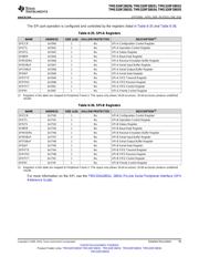
TMS320F28030
,
TMS320F28031
,
TMS320F28032
TMS320F28033
,
TMS320F28034
,
TMS320F28035
SPRS584K –APRIL 2009–REVISED JUNE 2016
www.ti.com
Submit Documentation Feedback
Product Folder Links: TMS320F28030 TMS320F28031 TMS320F28032 TMS320F28033 TMS320F28034
TMS320F28035
Detailed Description Copyright © 2009–2016, Texas Instruments Incorporated
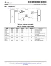
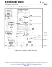
6.9.4 Serial Peripheral Interface (SPI) Module
The device includes the four-pin serial peripheral interface (SPI) module. Up to two SPI modules are
available. The SPI is a high-speed, synchronous serial I/O port that allows a serial bit stream of
programmed length (one to sixteen bits) to be shifted into and out of the device at a programmable bit-
transfer rate. Normally, the SPI is used for communications between the MCU and external peripherals or
another processor. Typical applications include external I/O or peripheral expansion through devices such
as shift registers, display drivers, and ADCs. Multidevice communications are supported by the
master/slave operation of the SPI.
The SPI module features include:
• Four external pins:
– SPISOMI: SPI slave-output/master-input pin
– SPISIMO: SPI slave-input/master-output pin
– SPISTE: SPI slave transmit-enable pin
– SPICLK: SPI serial-clock pin
NOTE: All four pins can be used as GPIO if the SPI module is not used.
• Two operational modes: master and slave
Baud rate: 125 different programmable rates.
• Data word length: one to sixteen data bits
• Four clocking schemes (controlled by clock polarity and clock phase bits) include:
– Falling edge without phase delay: SPICLK active-high. SPI transmits data on the falling edge of the SPICLK
signal and receives data on the rising edge of the SPICLK signal.
– Falling edge with phase delay: SPICLK active-high. SPI transmits data one half-cycle ahead of the falling edge
of the SPICLK signal and receives data on the falling edge of the SPICLK signal.
– Rising edge without phase delay: SPICLK inactive-low. SPI transmits data on the rising edge of the SPICLK
signal and receives data on the falling edge of the SPICLK signal.
– Rising edge with phase delay: SPICLK inactive-low. SPI transmits data one half-cycle ahead of the falling
edge of the SPICLK signal and receives data on the rising edge of the SPICLK signal.
• Simultaneous receive and transmit operation (transmit function can be disabled in software)
• Transmitter and receiver operations are accomplished through either interrupt-driven or polled algorithms.
• Nine SPI module control registers: Located in control register frame beginning at address 7040h.
NOTE
All registers in this module are 16-bit registers that are connected to Peripheral Frame 2.
When a register is accessed, the register data is in the lower byte (7–0), and the upper byte
(15–8) is read as zeros. Writing to the upper byte has no effect.
Enhanced feature:
• 4-level transmit/receive FIFO
• Delayed transmit control
• Bi-directional 3 wire SPI mode support
• Audio data receive support via SPISTE inversion
器件 Datasheet 文档搜索
AiEMA 数据库涵盖高达 72,405,303 个元件的数据手册,每天更新 5,000 多个 PDF 文件
