Datasheet 搜索 > 微控制器 > TI(德州仪器) > TMS320F28334ZJZQ 数据手册 > TMS320F28334ZJZQ 数据手册 79/195 页
 器件3D模型
¥ 158.047
TMS320F28334ZJZQ 数据手册 - TI(德州仪器)
制造商:
TI(德州仪器)
分类:
微控制器
封装:
BGA-176
描述:
数字信号控制器(DSC ) Digital Signal Controllers (DSCs)
Pictures:
3D模型
符号图
焊盘图
引脚图
产品图
页面导航:
引脚图在P15P80P81Hot
典型应用电路图在P49P96
原理图在P34P59P66P74P76P79P88P95P98P101P107
封装尺寸在P186P187P188
封装信息在P12P13P14P186P187P188
技术参数、封装参数在P46P47P117P118P119P120P121P122P123P124P125P126
应用领域在P62P114P140P195
电气规格在P47P117P118P119P120P121P122P123P124P125P126P127
导航目录
TMS320F28334ZJZQ数据手册
Page:
of 195 Go
若手册格式错乱,请下载阅览PDF原文件
ResultRegisters
EPWMSOCB
S/W
GPIO/
XINT2_ADCSOC
EPWMSOCA
S/W
Sequencer2
Sequencer1
SOCSOC
ADCControlRegisters
70B7h
70B0h
70AFh
70A8h
ResultReg15
ResultReg8
ResultReg7
ResultReg1
ResultReg0
12-Bit
ADC
Module
Analog
MUX
ADCINA0
ADCINA7
ADCINB0
ADCINB7
System
ControlBlock
High-Speed
Prescaler
HSPCLK
ADCENCLK
DSP
SYSCLKOUT
S/H
S/H
HALT
TMS320F28335, TMS320F28334, TMS320F28332
TMS320F28235, TMS320F28234, TMS320F28232
www.ti.com
SPRS439I–JUNE 2007–REVISED MARCH 2011
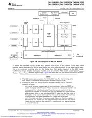
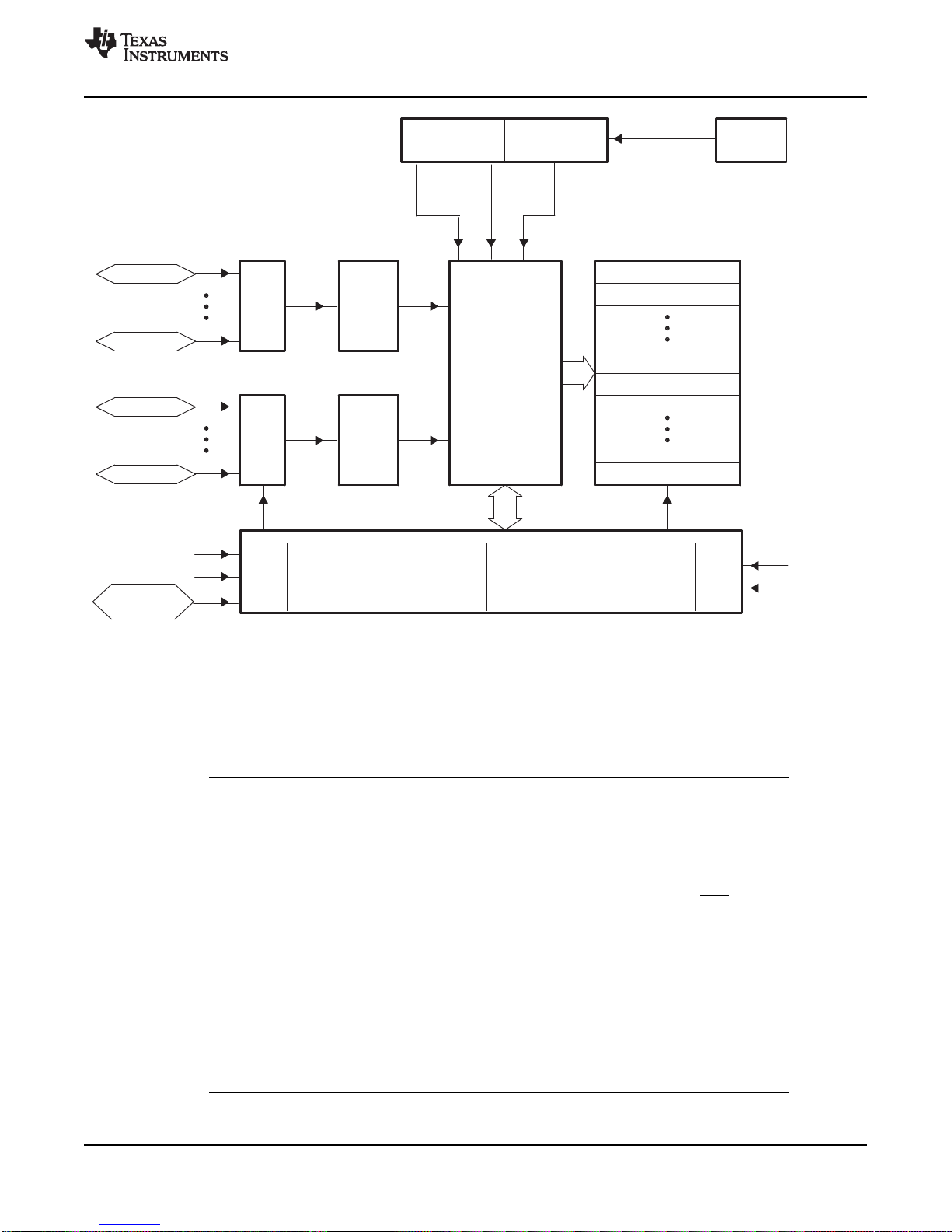
Figure 4-8. Block Diagram of the ADC Module
To obtain the specified accuracy of the ADC, proper board layout is very critical. To the best extent
possible, traces leading to the ADCIN pins should not run in close proximity to the digital signal paths.
This is to minimize switching noise on the digital lines from getting coupled to the ADC inputs.
Furthermore, proper isolation techniques must be used to isolate the ADC module power pins ( V
DD1A18
,
V
DD2A18
, V
DDA2
, V
DDAIO
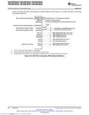
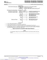
) from the digital supply.Figure 4-9 shows the ADC pin connections for the devices.
NOTE
1. The ADC registers are accessed at the SYSCLKOUT rate. The internal timing of the
ADC module is controlled by the high-speed peripheral clock (HSPCLK).
2. The behavior of the ADC module based on the state of the ADCENCLK and HALT
signals is as follows:
– ADCENCLK: On reset, this signal will be low. While reset is active-low (XRS) the
clock to the register will still function. This is necessary to make sure all registers and
modes go into their default reset state. The analog module, however, will be in a
low-power inactive state. As soon as reset goes high, then the clock to the registers
will be disabled. When the user sets the ADCENCLK signal high, then the clocks to
the registers will be enabled and the analog module will be enabled. There will be a
certain time delay (ms range) before the ADC is stable and can be used.
– HALT: This mode only affects the analog module. It does not affect the registers. In
this mode, the ADC module goes into low-power mode. This mode also will stop the
clock to the CPU, which will stop the HSPCLK; therefore, the ADC register logic will
be turned off indirectly.
Copyright © 2007–2011, Texas Instruments Incorporated Peripherals 79
Submit Documentation Feedback
Product Folder Link(s): TMS320F28335 TMS320F28334 TMS320F28332 TMS320F28235 TMS320F28234
TMS320F28232
Downloaded from Elcodis.com electronic components distributor
器件 Datasheet 文档搜索
AiEMA 数据库涵盖高达 72,405,303 个元件的数据手册,每天更新 5,000 多个 PDF 文件
