Datasheet 搜索 > 微控制器 > TI(德州仪器) > TMS320LF2406APZA 数据手册 > TMS320LF2406APZA 数据手册 57/134 页
 器件3D模型
¥ 30.487
TMS320LF2406APZA 数据手册 - TI(德州仪器)
制造商:
TI(德州仪器)
分类:
微控制器
封装:
LQFP-100
描述:
TEXAS INSTRUMENTS TMS320LF2406APZA 芯片, DSP, 16位 带闪存
Pictures:
3D模型
符号图
焊盘图
引脚图
产品图
页面导航:
引脚图在P61P62P63Hot
典型应用电路图在P55
原理图在P31P46P50P51P54P56P57P58P66
封装尺寸在P128
标记信息在P128P129
封装信息在P5P110P128P129
应用领域在P134
型号编号列表在P67
导航目录
TMS320LF2406APZA数据手册
Page:
of 134 Go
若手册格式错乱,请下载阅览PDF原文件

TMS320LF2407A,TMS320LF2406A,TMS320LF2403A,TMS320LF2402A
TMS320LC2406A,TMS320LC2404A,TMS320LC2403A,TMS320LC2402A
DSP CONTROLLERS
SPRS145L − JULY 2000 − REVISED SEPTEMBER 2007
57
POST OFFICE BOX 1443 • HOUSTON, TEXAS 77251−1443
SPI slave mode operation in LF2403A
The LF2403A device does not have the SPISTE
/IOPC5 pin. (This function is available as an internal signal only.)
The following must be done to put the LF2403A SPI in slave mode:
1. Configure SPISTE
/IOPC5 signal for GPIO mode by clearing the MCRB.5 bit.
2. Configure SPISTE
/IOPC5 signal as an output (by writing a 1 to bit 13 of PCDATDIR) and drive it low (by
writing a 0 to bit 5 of PCDATDIR). Note that SPISTE
/IOPC5 should not be driven low until after the SPI is
configured and taken out of reset.
NOTE: The slave SPISTE
/IOPC5 signal must not be driven low until after the master and slave SPI modules
are configured and taken out of reset. The initialization sequence is as follows:
a. The master SPI is configured first and taken out of reset. This ensures that the master SPICLK is
initialized to its appropriate level (high or low, depending on the polarity bit) first, before the slave SPI
starts accepting clock pulses.
b. The slave SPI is configured and taken out of reset.
c. The GPIO/SPI pins of the slave is then configured for SPI operation and the SPISTE
/IOPC5 signal is
driven low. This is done after ensuring the correct level of the master SPICLK signal. One method of
doing this would be to read the level of the SPICLK pin through the PCDATDIR register and then
deciding on the appropriate course of action.
d. SPI transmission may commence now. Transmission of data should not be attempted until both master
and slave are configured and the slave SPISTE
/IOPC5 signal is driven low.
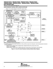
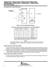
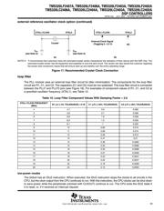
PLL-based clock module
The 240xA has an on-chip, PLL-based clock module. This module provides all the necessary clocking signals
for the device, as well as control for low-power mode entry. The PLL has a 3-bit ratio control to select different
CPU clock rates. See Figure 16 for the PLL Clock Module Block Diagram, Table 9 for clock rates, and Table 10
for the loop filter component values.
The PLL-based clock module provides two modes of operation:
D Crystal-operation
This mode allows the use of an external crystal/resonator to provide the time base to the device.
D External clock source operation
This mode allows the internal oscillator to be bypassed. The device clocks are generated from an external
clock source input on the XTAL1/CLKIN pin. In this case, an external oscillator clock is connected to the
XTAL1/CLKIN pin.
器件 Datasheet 文档搜索
AiEMA 数据库涵盖高达 72,405,303 个元件的数据手册,每天更新 5,000 多个 PDF 文件
