Datasheet 搜索 > DSP数字信号处理器 > TI(德州仪器) > TMS320VC5402PGER10 数据手册 > TMS320VC5402PGER10 数据手册 1/72 页
 器件3D模型
¥ 85.763
TMS320VC5402PGER10 数据手册 - TI(德州仪器)
制造商:
TI(德州仪器)
分类:
DSP数字信号处理器
封装:
LQFP-144
描述:
定点数字信号处理器 FIXED-POINT DIGITAL SIGNAL PROCESSOR
Pictures:
3D模型
符号图
焊盘图
引脚图
产品图
页面导航:
导航目录
TMS320VC5402PGER10数据手册
Page:
of 72 Go
若手册格式错乱,请下载阅览PDF原文件

SPRS079G − OCTOBER 1998 − REVISED OCTOBER 2008
1
POST OFFICE BOX 1443 • HOUSTON, TEXAS 77251−1443
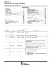
D Advanced Multibus Architecture With Three
Separate 16-Bit Data Memory Buses and
One Program Memory Bus
D 40-Bit Arithmetic Logic Unit (ALU),
Including a 40-Bit Barrel Shifter and Two
Independent 40-Bit Accumulators
D 17- × 17-Bit Parallel Multiplier Coupled to a
40-Bit Dedicated Adder for Non-Pipelined
Single-Cycle Multiply/Accumulate (MAC)
Operation
D Compare, Select, and Store Unit (CSSU) for
the Add/Compare Selection of the Viterbi
Operator
D Exponent Encoder to Compute an
Exponent Value of a 40-Bit Accumulator
Value in a Single Cycle
D Two Address Generators With Eight
Auxiliary Registers and Two Auxiliary
Register Arithmetic Units (ARAUs)
D Data Bus With a Bus-Holder Feature
D Extended Addressing Mode for 1M × 16-Bit
Maximum Addressable External Program
Space
D 4K x 16-Bit On-Chip ROM
D 16K x 16-Bit Dual-Access On-Chip RAM
D Single-Instruction-Repeat and
Block-Repeat Operations for Program Code
D Block-Memory-Move Instructions for
Efficient Program and Data Management
D Instructions With a 32-Bit Long Word
Operand
D Instructions With Two- or Three-Operand
Reads
D Arithmetic Instructions With Parallel Store
and Parallel Load
D Conditional Store Instructions
D Fast Return From Interrupt
D On-Chip Peripherals
− Software-Programmable Wait-State
Generator and Programmable Bank
Switching
− On-Chip Phase-Locked Loop (PLL) Clock
Generator With Internal Oscillator or
External Clock Source
− Two Multichannel Buffered Serial Ports
(McBSPs)
− Enhanced 8-Bit Parallel Host-Port
Interface (HPI8)
− Two 16-Bit Timers
− Six-Channel Direct Memory Access
(DMA) Controller
D Power Consumption Control With IDLE1,
IDLE2, and IDLE3 Instructions With
Power-Down Modes
D CLKOUT Off Control to Disable CLKOUT
D On-Chip Scan-Based Emulation Logic,
IEEE Std 1149.1
†
(JTAG) Boundary Scan
Logic
D 10-ns Single-Cycle Fixed-Point Instruction
Execution Time (100 MIPS) for 3.3-V Power
Supply (1.8-V Core)
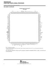
D Available in a 144-Pin Plastic Low-Profile
Quad Flatpack (LQFP) (PGE Suffix) and a
144-Pin Ball Grid Array (BGA) (GGU Suffix)
NOTE:This data sheet is designed to be used in conjunction with the TMS320C5000 DSP Family Functional Overview
(literature number SPRU307).
Copyright 2008, Texas Instruments Incorporated
Please be aware that an important notice concerning availability, standard warranty, and use in critical applications o
f
Texas Instruments semiconductor products and disclaimers thereto appears at the end of this data sheet.
All trademarks are the property of their respective owners.
†
IEEE Standard 1149.1-1990 Standard-Test-Access Port and Boundary Scan Architecture.
! " #$%! " &$'(#! )!%*
)$#!" # ! "&%##!" &% !+% !%" %," "!$%!"
"!)) -!.* )$#! &#%""/ )%" ! %#%""(. #($)%
!%"!/ (( &%!%"*
器件 Datasheet 文档搜索
AiEMA 数据库涵盖高达 72,405,303 个元件的数据手册,每天更新 5,000 多个 PDF 文件
