Datasheet 搜索 > DC/DC转换器 > TI(德州仪器) > TPS2412PWR 数据手册 > TPS2412PWR 数据手册 4/29 页
 器件3D模型
¥ 1.157
TPS2412PWR 数据手册 - TI(德州仪器)
制造商:
TI(德州仪器)
分类:
DC/DC转换器
封装:
TSSOP-8
描述:
N1和的ORing电源导轨控制器 N1 and ORing Power Rail Controller
Pictures:
3D模型
符号图
焊盘图
引脚图
产品图
页面导航:
引脚图在P3Hot
典型应用电路图在P1P10P11P14P15
原理图在P9
封装尺寸在P20P22P23P24
焊盘布局在P18P25
标记信息在P20P21
封装信息在P19P20P21P22P23
技术参数、封装参数在P4
应用领域在P1P14P29
电气规格在P5


导航目录
TPS2412PWR数据手册
Page:
of 29 Go
若手册格式错乱,请下载阅览PDF原文件
TPS2412
,
TPS2413
SLVS728C –JANUARY 2007–REVISED NOVEMBER 2015
www.ti.com
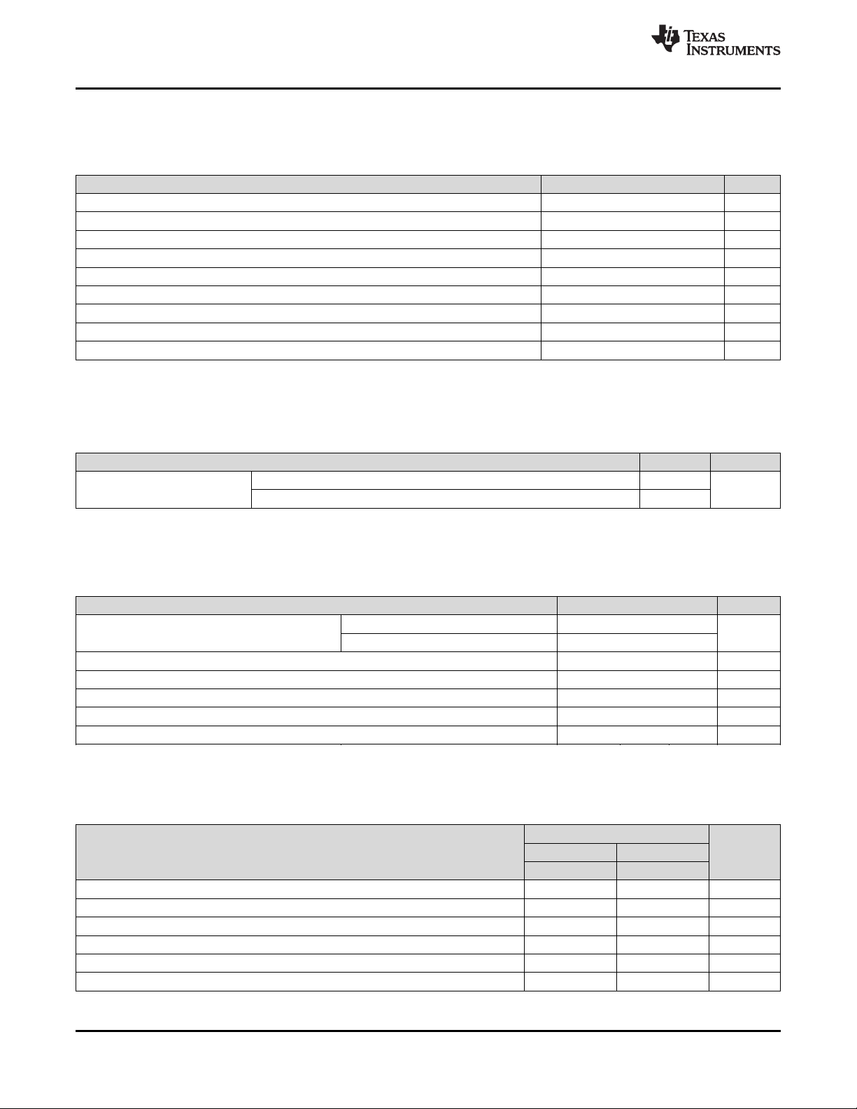
7 Specifications
7.1 Absolute Maximum Ratings
over operating free-air temperature range, voltage are referenced to GND (unless otherwise noted)
(1)
MIN MAX UNIT
A, C, FLTR, V
DD
, voltage –0.3 18 V
A above C voltage 7.5 V
C above A voltage 18 V
GATE
(2)
, BYP voltage –0.3 30 V
BYP to A voltage –0.3 13 V
GATE above BYP
(2)
voltage 0.3 V
RSET
(2)
voltage –0.3 7 V
GATE short to A or C or GND Indefinite
T
J
Maximum junction temperature Internally limited °C
(1) Stresses beyond those listed under Absolute Maximum Ratings may cause permanent damage to the device. These are stress ratings
only and functional operation of the device at these or any other conditions beyond those indicated under Recommended Operating
Conditions is not implied. Exposure to absolute-maximum-rated conditions for extended periods may affect device reliability.
(2) Voltage should not be applied to these pins.
7.2 ESD Ratings
VALUE UNIT
Human-body model (HBM), per ANSI/ESDA/JEDEC JS-001
(1)
±2000
V
(ESD)
Electrostatic discharge V
Charged-device model (CDM), per JEDEC specification JESD22-C101
(2)
±500
(1) JEDEC document JEP155 states that 500-V HBM allows safe manufacturing with a standard ESD control process.
(2) JEDEC document JEP157 states that 250-V CDM allows safe manufacturing with a standard ESD control process.
7.3 Recommended Operating Conditions
voltages are referenced to GND (unless otherwise noted)
MIN NOM MAX UNIT
V
DD
= V
(C)
(1)
3 16.5
A, C Input voltage range TPS2412 V
3 ≤ V
DD
≤ 16.5 V 0.8 16.5
A to C Operational voltage 5 V
R
(RSET)
Resistance range
(2)
1.5 ∞ kΩ
C
(BYP)
Capacitance Range
(2) (3)
800 2200 10k pF
T
J
Operating junction temperature –40 125 °C
T
A
Operating free-air temperature –40 85 °C
(1) V
DD
must exceed 3 V to meet gate drive specification
(2) Voltage should not be applied to these pins.
(3) Capacitors should be X7R, 20% or better
7.4 Thermal Information
TPS241x
THERMAL METRIC
(1)
PW (TSSOP) D (SOIC) UNIT
8 PINS 8 PINS
R
θJA
Junction-to-ambient thermal resistance 110.3 110.3 °C/W
R
θJC(top)
Junction-to-case (top) thermal resistance 54.7 54.7 °C/W
R
θJB
Junction-to-board thermal resistance 50.9 50.9 °C/W
ψ
JT
Junction-to-top characterization parameter 9.2 9.2 °C/W
ψ
JB
Junction-to-board characterization parameter 50.4 50.4 °C/W
R
θJC(bot)
Junction-to-case (bottom) thermal resistance N/A N/A °C/W
(1) For more information about traditional and new thermal metrics, see the Semiconductor and IC Package Thermal Metrics application
report, SPRA953.
4 Submit Documentation Feedback Copyright © 2007–2015, Texas Instruments Incorporated
Product Folder Links: TPS2412 TPS2413
器件 Datasheet 文档搜索
AiEMA 数据库涵盖高达 72,405,303 个元件的数据手册,每天更新 5,000 多个 PDF 文件
