Datasheet 搜索 > TI(德州仪器) > TPS54308DDCR 数据手册 > TPS54308DDCR 数据手册 8/28 页

¥ 1.889
TPS54308DDCR 数据手册 - TI(德州仪器)
制造商:
TI(德州仪器)
封装:
TSOT-23-6
描述:
TPS54308DDCR 编带
Pictures:
3D模型
符号图
焊盘图
引脚图
产品图
页面导航:
导航目录
TPS54308DDCR数据手册
Page:
of 28 Go
若手册格式错乱,请下载阅览PDF原文件
FB
Voltage
Reference
HS MOSFET
Current
Comparator
Slope
Compensation
Overload
Recovery
Maximum
Clamp
Oscillator
Power Stage
and Dead Time
Control Logic
LS MOSFET
Current Limit
Overvoltage
Comparator
Boot
UVLO
Regulator
V
IN
Boot Charge
GND
BOOT
SW
Current
Sense
Current
Sense
IN
I
h
I
p
EN
Enable
Comparator
Shutdown
Logic
Thermal Hiccup
UVLO
Hiccup
Shutdown
Hiccup
Shutdown
+
±
+
±
+
Soft Start
2.04 nF
20 k
Error
Amplifier
2 pF
Copyright © 2017, Texas Instruments Incorporated
8
TPS54308
SLUSCV2 –JUNE 2017
www.ti.com
Product Folder Links: TPS54308
Submit Documentation Feedback Copyright © 2017, Texas Instruments Incorporated
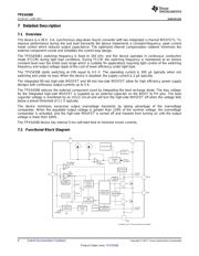
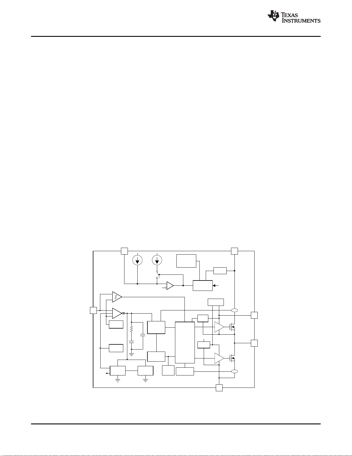
7 Detailed Description
7.1 Overview
The device is a 28-V, 3-A, synchronous step-down (buck) converter with two integrated n-channel MOSFETs. To
improve performance during line and load transients the device implements a constant-frequency, peak current
mode control which reduces output capacitance. The optimized internal compensation network minimizes the
external component counts and simplifies the control loop design.
The TPS54308’s switching frequency is fixed to 350 kHz, and this device operates in continuous conduction
mode (FCCM) during light load conditions. During FCCM, the switching frequency is maintained at an almost
constant level over the entire load range which is suitable fro applications requiring tight control of the switching
frequency and output voltage ripple at the cost of lower efficiency under light load.
The TPS54308 starts switching at VIN equal to 4.5 V. The operating current is 300 μA typically when not
switching and under no load. When the device is disabled, the supply current is 2 µA typically.
The integrated 85-mΩ high-side MOSFET and 40-mΩ low-side MOSFET allow for high efficiency power supply
designs with continuous output currents up to 3 A.
The TPS54308 reduces the external component count by integrating the boot recharge diode. The bias voltage
for the integrated high-side MOSFET is supplied by an external capacitor on the BOOT to PH pins. The boot
capacitor voltage is monitored by an UVLO circuit and will turn the high-side MOSFET off when the voltage falls
below a preset threshold of 2.1 V typically.
The device minimizes excessive output overvoltage transients by taking advantage of the overvoltage
comparator. When the regulated output voltage is greater than 118% of the nominal voltage, the overvoltage
comparator is activated, and the high-side MOSFET is turned off and masked from turning on until the output
voltage is lower than 104%.
The TPS54308 device has internal 5-ms soft-start time to minimize inrush currents.
7.2 Functional Block Diagram
器件 Datasheet 文档搜索
AiEMA 数据库涵盖高达 72,405,303 个元件的数据手册,每天更新 5,000 多个 PDF 文件
