Datasheet 搜索 > DC/DC转换器 > TI(德州仪器) > TPS62080ADSGT 数据手册 > TPS62080ADSGT 数据手册 16/27 页

¥ 6.669
TPS62080ADSGT 数据手册 - TI(德州仪器)
制造商:
TI(德州仪器)
分类:
DC/DC转换器
封装:
WSON-8
描述:
6V,TPS 系列,Texas Instruments### 直流/直流开关调节器转换器(集成开关),Texas InstrumentsTexas Instruments 的此系列高度集成的高效开关稳压器包括步升(升压)、步降(降压)、步升/降(增压/降压)和反相类型,为每个直流稳压器应用提供高效的解决方案。
Pictures:
3D模型
符号图
焊盘图
引脚图
产品图
页面导航:
引脚图在P4Hot
典型应用电路图在P1P10P11P16P17
原理图在P5
封装尺寸在P20P22P23
型号编码规则在P2
标记信息在P2P20P21
封装信息在P2P20P21P22P23
技术参数、封装参数在P2
应用领域在P1P27
电气规格在P3
导航目录
TPS62080ADSGT数据手册
Page:
of 27 Go
若手册格式错乱,请下载阅览PDF原文件
÷
ø
ö
ç
è
æ
+´=
÷
ø
ö
ç
è
æ
+´=
2R
1R
1V45.0
2R
1R
1VV
FBOUT
TPS62080
1mH
10µF
2.3V .. 6V
R
1
R
2
V
IN
POWER GOOD
SW
VOS
VIN
EN
GND
MODE
PG
FB
22µF
180k
V
OUT
TPS62080, TPS62080A
TPS62081, TPS62082
SLVSAE8D –SEPTEMBER 2011–REVISED JULY 2013
www.ti.com
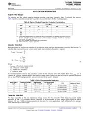
The architecture of the TPS6208X allows to use tiny ceramic-type output capacitors with low equivalent series
resistance (ESR). These capacitors provide low output voltage ripple and are recommended. To keep its
resistance up to high frequencies and to get narrow capacitance variation with temperature, it's recommended to
use X7R or X5R dielectric. The TPS6208x is designed to operate with an output capacitance of 10µF to 100µF,
as outlined in Table 4.
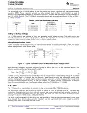
Table 6. List of Recommended Capacitors
CAPACITANCE DIMENSIONS
TYPE MANUFACTURER
[µF] L x W x H [mm
3
]
10 GRM188R60J106M 0603: 1.6 x 0.8 x 0.8 Murata
22 GRM188R60G226M 0603: 1.6 x 0.8 x 0.8 Murata
22 GRM21BR60J226M 0805: 2.0 x 1.2 x 1.25 Murata
Setting the Output Voltage
The TPS608x devices are available as fixed and adjustable output voltage versions. The fixed versions are
internally programmed to a fixed output voltage, whereas the adjustable output voltage version needs to be
programmed via an external voltage divider to set the desired output voltage.
Adjustable output voltage version
For the adjustable output voltage version, an external resistor divider is used. By selecting R
1
and R
2
, the output
voltage is programmed to the desired value.
Figure 31. Typical Application Circuit for Adjustable Output Voltage Option
When the output voltage is regulated, the typical voltage at the FB pin is V
FB
for the adjustable devices. The
following equation can be used to calculate R
1
and R
2
.
(3)
For best accuracy, R2 should be kept smaller than 40kΩ to ensure that the current flowing through R2 is at least
100 times larger than I
FB
. Changing the sum towards a lower value increases the robustness against noise
injection. Changing the sum towards higher values reduces the quiescent current and supports the Snooze Mode
function for achieving highest efficiency at low load currents. For lowest quiescent current during the Snooze
Mode, it is recommended to use a fixed output voltage version like TPS62081 and TPS62082.
PCB Layout
The PCB layout is an important step to maintain the high performance of the TPS6208x devices.
The input/output capacitors and the inductor should be placed as close as possible to the IC. This keeps the
traces short. Routing these traces direct and wide results in low trace resistance and low parasitic inductance. A
common power GND should be used. The low side of the input and output capacitors must be connected
properly to the power GND to avoid a GND potential shift.
The sense traces connected to FB and VOS pins are signal traces. Special care should be taken to avoid noise
being induced. By a direct routing, parasitic inductance can be kept small. GND layers might be used for
shielding. Keep these traces away from SW nodes.
16 Submit Documentation Feedback Copyright © 2011–2013, Texas Instruments Incorporated
Product Folder Links: TPS62080 TPS62080A TPS62081 TPS62082
器件 Datasheet 文档搜索
AiEMA 数据库涵盖高达 72,405,303 个元件的数据手册,每天更新 5,000 多个 PDF 文件
