Datasheet 搜索 > 稳压芯片 > TI(德州仪器) > TPS70950DBVR 数据手册 > TPS70950DBVR 数据手册 15/34 页

¥ 0.981
TPS70950DBVR 数据手册 - TI(德州仪器)
制造商:
TI(德州仪器)
分类:
稳压芯片
封装:
SOT-23-5
描述:
TEXAS INSTRUMENTS TPS70950DBVR 芯片, 稳压器, LDO, 固定, 0.15A, 5V, SOT-23-5 新
Pictures:
3D模型
符号图
焊盘图
引脚图
产品图
页面导航:
引脚图在P4Hot
典型应用电路图在P1P15
原理图在P13
封装尺寸在P20P21P22P23P25P26P27P28
标记信息在P20P21P22P23
封装信息在P18P19P20P21P22P23P24P25P26P27P28
技术参数、封装参数在P5
应用领域在P1P34
电气规格在P6
导航目录
TPS70950DBVR数据手册
Page:
of 34 Go
若手册格式错乱,请下载阅览PDF原文件
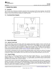
TPS70933
EN
IN
OUT
V
IN
V
OUT
1 Fm
2.2 Fm
GND
NC
TPS709
www.ti.com
SBVS186G –MARCH 2012–REVISED NOVEMBER 2015
8 Application and Implementation
NOTE
Information in the following applications sections is not part of the TI component
specification, and TI does not warrant its accuracy or completeness. TI’s customers are
responsible for determining suitability of components for their purposes. Customers should
validate and test their design implementation to confirm system functionality.
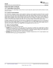
8.1 Application Information
The TPS709 is a series of devices that belong to a new family of next-generation voltage regulators. These
devices consume low quiescent current and deliver excellent line and load transient performance. This
performance, combined with low noise and very good PSRR with little (V
IN
– V
OUT
) headroom, makes these
devices ideal for RF portable applications, current limit, and thermal protection. The TPS709 is specified from
–40°C to +125°C.
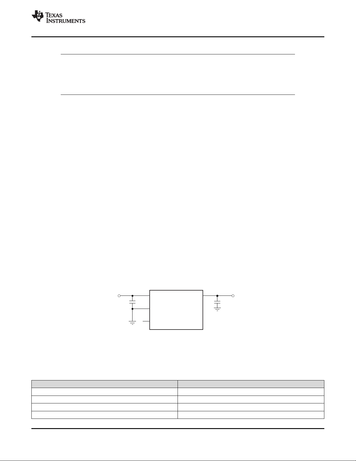
8.1.1 Input and Output Capacitor
The TPS709 devices are stable with output capacitors with an effective capacitance of 2.0 μF or greater for
output voltages below 1.5 V. For output voltages equal or greater than 1.5 V, the minimum effective capacitance
for stability is 1.5 µF. The maximum capacitance for stability is 47 µF. The equivalent series resistance (ESR) of
the output capacitor must be between 0 Ω and 0.2 Ω for stability.
The effective capacitance is the minimum capacitance value of a capacitor after taking into account variations
resulting from tolerances, temperature, and dc bias effects. X5R- and X7R-type ceramic capacitors are
recommended because these capacitors have minimal variation in value and ESR over temperature.
Although an input capacitor is not required for stability, good analog design practice is to connect a 0.1-µF to
2.2-µF capacitor from IN to GND. This capacitor counteracts reactive input sources and improves transient
response, input ripple, and PSRR. An input capacitor is necessary if line transients greater than 10 V in
magnitude are anticipated.
8.1.2 Transient Response
As with any regulator, increasing the output capacitor size reduces over- and undershoot magnitude, but
increases transient response duration.
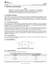
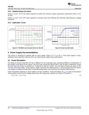
8.2 Typical Application
Figure 36. Wide Input, 3.3-V, Low-I
Q
Rail
8.2.1 Design Requirements
Table 1 summarizes the design requirements for Figure 36.
Table 1. Design Requirements for a Wide Input, 3.3-V, Low-I
Q
Rail Application
PARAMETER DESIGN SPECIFICATION
V
IN
5 V to 20 V
V
OUT
3.3 V
I
(IN)
(no load) < 5 µA
I
OUT
(max) 150 mA
Copyright © 2012–2015, Texas Instruments Incorporated Submit Documentation Feedback 15
Product Folder Links: TPS709
器件 Datasheet 文档搜索
AiEMA 数据库涵盖高达 72,405,303 个元件的数据手册,每天更新 5,000 多个 PDF 文件
