Datasheet 搜索 > 稳压芯片 > TI(德州仪器) > TPS767D301PWP 数据手册 > TPS767D301PWP 数据手册 2/22 页
 器件3D模型
¥ 3.677
TPS767D301PWP 数据手册 - TI(德州仪器)
制造商:
TI(德州仪器)
分类:
稳压芯片
封装:
HTSSOP-28
描述:
LDO(低压降)线性稳压器,1A,TPS系列,Texas Instruments### LDO(低压降)线性电压调节器,Texas Instruments低压降或 LDO 为线性电压稳压器。 我们有多种系列的线性稳压器。 LDO 稳压器可在输入 - 输出差分电压较小时运行。 LDO 电压稳压器可提供快速瞬态响应、宽输入电压范围、低静态电流、低噪声、高 PSRR。
Pictures:
3D模型
符号图
焊盘图
引脚图
产品图
页面导航:
封装尺寸在P15P17P18
标记信息在P15P16
封装信息在P15P16P17P18
应用领域在P16P22
导航目录
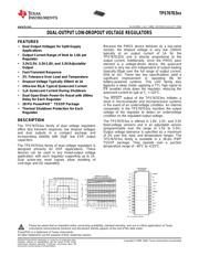
TPS767D301PWP数据手册
Page:
of 22 Go
若手册格式错乱,请下载阅览PDF原文件
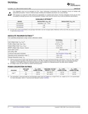
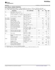
ABSOLUTE MAXIMUM RATINGS
(1)
POWER DISSIPATION RATINGS
TPS767D3xx
SLVS209H – JULY 1999 – REVISED AUGUST 2008 .........................................................................................................................................................
www.ti.com
This integrated circuit can be damaged by ESD. Texas Instruments recommends that all integrated circuits be handled with
appropriate precautions. Failure to observe proper handling and installation procedures can cause damage.
ESD damage can range from subtle performance degradation to complete device failure. Precision integrated circuits may be more
susceptible to damage because very small parametric changes could cause the device not to meet its published specifications.
AVAILABLE OPTIONS
(1)
DEVICE REGULATOR 1 V
OUT
(V) REGULATOR 2 V
OUT
(V)
TPS767D301 Adjustable (1.5V – 5.5V) 3.3V
TPS767D318 1.8V 3.3V
TPS767D325 2.5V 3.3V
(1) For the most current specifications and package information see the Package Option Addendum at the end of this document, or see the
TI web site at www.ti.com.
Over operating temperature range (unless otherwise noted).
TPS767D3xx UNIT
Input voltage range, V
1IN
, V
2IN
(2)
– 0.3 to +13.5 V
Enable voltage range, V
1EN
, V
2EN
– 0.3 to V
IN
+ 0.3 V
Output voltage range, V
1OUT
, V
2OUT
– 0.3 to +7.0 V
RESET voltage range, V
1RESET
, V
2RESET
– 0.3 to +16.5 V
Peak output current Internally limited
ESD rating, HBM 2 kV
Continuous total power dissipation See Dissipation Ratings table
Operating junction temperature range, T
J
– 40 to +125 ° C
Storage temperature range, T
stg
– 65 to +150 ° C
(1) Stresses beyond those listed under absolute maximum ratings may cause permanent damage to the device. These are stress ratings
only, and functional operation of the device at these or any other conditions beyond those indicated under recommended operating
conditions is not implied. Exposure to absolute-maximum-rated conditions for extended periods may affect device reliability.
(2) All voltage values are with respect to network terminal ground.
AIR FLOW T
A
≤ +25 ° C DERATING FACTOR T
A
= +70 ° C T
A
= +85 ° C
PACKAGE (CFM) POWER RATING ABOVE t
a
= +25 ° C POWER RATING POWER RATING
0 3.58 W 35.8 mW/ ° C 1.97 W 1.43 W
PWP
(1)
250 5.07 W 50.7 mW/ ° C 2.79 W 2.03 W
(1) This parameter is measured with the recommended copper heat sink pattern on a 4-layer PCB, 1oz. copper on 4-in × 4-in ground layer.
For more information, refer to TI technical brief literature number SLMA002 .
2 Submit Documentation Feedback Copyright © 1999 – 2008, Texas Instruments Incorporated
器件 Datasheet 文档搜索
AiEMA 数据库涵盖高达 72,405,303 个元件的数据手册,每天更新 5,000 多个 PDF 文件
