Datasheet 搜索 > 稳压芯片 > TI(德州仪器) > TPS7A4501DCQT 数据手册 > TPS7A4501DCQT 数据手册 13/36 页
¥ 7.775
TPS7A4501DCQT 数据手册 - TI(德州仪器)
制造商:
TI(德州仪器)
分类:
稳压芯片
封装:
SOT-223-6
描述:
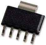
TEXAS INSTRUMENTS TPS7A4501DCQT 电压稳压器, LDO, 可调, 2.1V至20V输入, 300mV压差, 1.21V至20V/1.5A输出, SOT-223-5
Pictures:
3D模型
符号图
焊盘图
引脚图
产品图
页面导航:
引脚图在P3Hot
典型应用电路图在P18
原理图在P1P13
封装尺寸在P27P28P30P31
标记信息在P27P28
封装信息在P26P27P28P29P30P31
技术参数、封装参数在P4P18
应用领域在P1P18P29P36
电气规格在P4P5P6P7
导航目录
TPS7A4501DCQT数据手册
Page:
of 36 Go
若手册格式错乱,请下载阅览PDF原文件
IN
SHDN
OUT
SENSE/ADJ
GND
+
Reverse
Current
Protection
Pass
Element
Current
Limit
Error Amplifier
Voltage Reference
+
Thermal
Overload
Reverse
Voltage
Protection
TPS7A4501
,
TPS7A4515
,
TPS7A4518
,
TPS7A4525
,
TPS7A4533
www.ti.com
SLVS720F –JUNE 2008–REVISED NOVEMBER 2015
8 Detailed Description
8.1 Overview
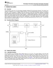
The TPS7A45xx series are 1.5-A low-dropout regulators optimized for fast transient response. The devices are
capable of supplying 1.5 A at a dropout voltage of 300 mV. The low operating quiescent current (1 mA) drops to
less than 1 μA in shutdown. In addition to the low quiescent current, the TPS7A45xx regulators incorporate
several protection features that make them ideal for use in battery-powered systems. The devices are protected
against both reverse input and reverse output voltages. In battery-backup applications where the output can be
held up by a backup battery when the input is pulled to ground, the TPS7A45xx acts as if it has a diode in series
with its output and prevents reverse current flow. Additionally, in dual-supply applications where the regulator
load is returned to a negative supply, the output can be pulled below ground by as much as (20 V – VIN) and still
allow the device to start and operate.
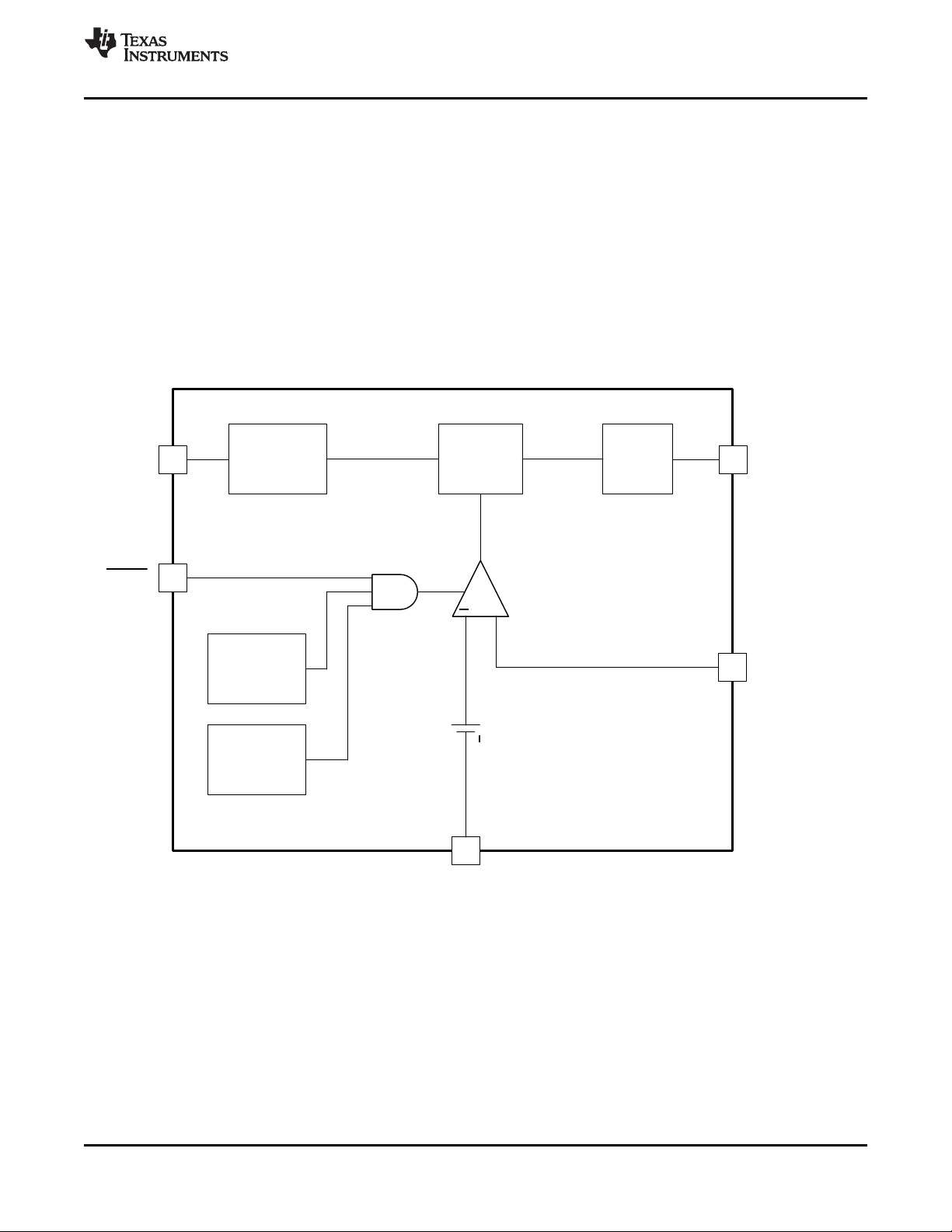
8.2 Functional Block Diagram
8.3 Feature Description
8.3.1 Adjustable Operation
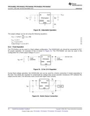
The TPS7A4501 has an adjustable output voltage range of 1.21 V to 20 V. The output voltage is set by the ratio
of two external resistors as shown in Figure 30. The device maintains the voltage at the ADJ pin at 1.21 V
referenced to ground. The current in R1 is then equal to (1.21 V/R1), and the current in R2 is the current in R1
plus the ADJ pin bias current. The ADJ pin bias current, 3 μA at 25°C, flows through R2 into the ADJ pin. The
output voltage can be calculated using the formula shown in Equation 1. The value of R1 should be less than
4.17 kΩ to minimize errors in the output voltage caused by the ADJ pin bias current. Note that in shutdown the
output is turned off, and the divider current is zero.
Copyright © 2008–2015, Texas Instruments Incorporated Submit Documentation Feedback 13
Product Folder Links: TPS7A4501 TPS7A4515 TPS7A4518 TPS7A4525 TPS7A4533
器件 Datasheet 文档搜索
AiEMA 数据库涵盖高达 72,405,303 个元件的数据手册,每天更新 5,000 多个 PDF 文件

