Datasheet 搜索 > 稳压芯片 > TI(德州仪器) > TPS7A6550QKVURQ1 数据手册 > TPS7A6550QKVURQ1 数据手册 2/18 页

¥ 5.035
TPS7A6550QKVURQ1 数据手册 - TI(德州仪器)
制造商:
TI(德州仪器)
分类:
稳压芯片
封装:
TO-252-3
描述:
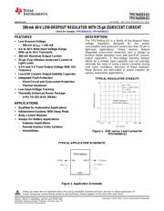
TEXAS INSTRUMENTS TPS7A6550QKVURQ1 固定电压稳压器, LDO, 5.3V至40V, 300mV压差, 5V输出, 300mA输出, TO-252AA-3
Pictures:
3D模型
符号图
焊盘图
引脚图
产品图
页面导航:
典型应用电路图在P1P10
原理图在P1P4P10
封装尺寸在P13P14P15
型号编码规则在P2
标记信息在P2P13
封装信息在P2P13P14P15
技术参数、封装参数在P2
应用领域在P1P18
电气规格在P3
导航目录
TPS7A6550QKVURQ1数据手册
Page:
of 18 Go
若手册格式错乱,请下载阅览PDF原文件
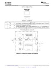
TPS7A6533-Q1
TPS7A6550-Q1
SLVSA98C –MAY 2010–REVISED JULY 2012
www.ti.com
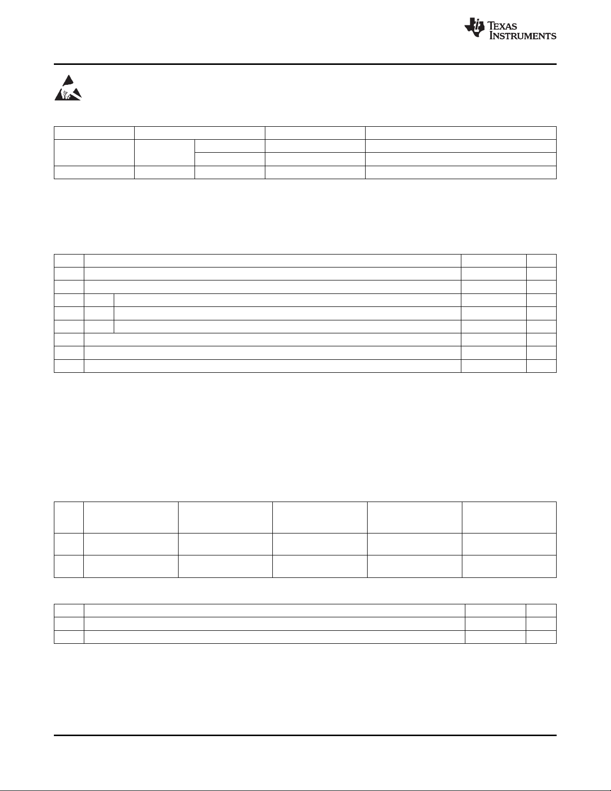
These devices have limited built-in ESD protection. The leads should be shorted together or the device placed in conductive foam
during storage or handling to prevent electrostatic damage to the MOS gates.
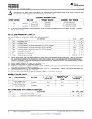
ORDERING INFORMATION
(1)
OUTPUT VOLTAGE PACKAGE TOP-SIDE MARKING ORDERABLE PART NUMBER
Tube of 70 7A6550Q1 TPS7A6550QKVUQ1
5 V 3-pin KVU
Reel of 2500 7A6550Q1 TPS7A6550QKVURQ1
3.3 V 3-pin KVU Reel of 2500 7A6533Q1 TPS7A6533QKVURQ1
(1) For the most-current package and ordering information, see the Package Option Addendum at the end of this document, or see the TI
Web site at www.ti.com.
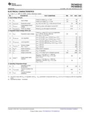
ABSOLUTE MAXIMUM RATINGS
(1)
over operating free-air temperature range (unless otherwise noted)
NO. DESCRIPTION VALUE UNIT
1.1 V
IN
Unregulated input
(2)(3)
45 V
1.2 V
OUT
Regulated output 7 V
1.3 θ
JP
Thermal impedance junction to exposed pad KVU (DPAK) package 1.2 °C/W
1.4 θ
JA
Thermal impedance junction to ambient KVU (DPAK) package
(4)
29.3 °C/W
1.5 θ
JA
Thermal impedance junction to ambient KVU (DPAK) package
(5)
38.6 °C/W
1.6 ESD Electrostatic discharge
(6)
2 kV
1.7 T
A
Operating ambient temperature 125 °C
1.8 T
stg
Storage temperature range –65 to 150 °C
(1) Stresses beyond those listed under Absolute Maximum Ratings may cause permanent damage to the device. These are stress ratings
only, and functional operation of the device at these or any other conditions beyond those indicated under Recommended Operating
Conditions is not implied. Exposure to absolute-maximum-rated conditions for extended periods may affect device reliability. All voltage
values are with respect to GND.
(2) Absolute negative voltage on these pins not to go below –0.3 V.
(3) Absolute maximum voltage for duration less than 480 ms.
(4) The thermal data is based on JEDEC standard high-K profile – JESD 51-5. The copper pad is soldered to the thermal land pattern. Also
correct attachment procedure must be incorporated.
(5) The thermal data is based on JEDEC standard low-K profile – JESD 51-3. The copper pad is soldered to the thermal land pattern. Also
correct attachment procedure must be incorporated.
(6) The human-body model is a 100-pF capacitor discharged through a 1.5-kΩ resistor into each pin.
DISSIPATION RATINGS
DERATING FACTOR
T
A
< 25°C POWER T
A
= 85°C POWER
NO. JEDEC STANDARD PACKAGE ABOVE T
A
= 25°C
RATING (W) RATING (W)
(°C/W)
JEDEC Standard PCB -
2.1 3 pin KVU 3.24 38.6 1.68
low K, JESD 51-3
JEDEC Standard PCB -
2.2 3 pin KVU 4.27 29.3 2.22
high K, JESD 51-5
RECOMMENDED OPERATING CONDITIONS
NO. DESCRIPTION MIN MAX UNIT
3.1 V
IN
Unregulated input voltage 4 40 V
3.2 T
J
Operating junction temperature range –40 150 °C
2 Submit Documentation Feedback Copyright © 2010–2012, Texas Instruments Incorporated
Product Folder Link(s): TPS7A6533-Q1 TPS7A6550-Q1
器件 Datasheet 文档搜索
AiEMA 数据库涵盖高达 72,405,303 个元件的数据手册,每天更新 5,000 多个 PDF 文件
