Datasheet 搜索 > VISHAY(威世) > TPSMA33AHE3/5AT 数据手册 > TPSMA33AHE3/5AT 数据手册 1/5 页

¥ 0
TPSMA33AHE3/5AT 数据手册 - VISHAY(威世)
制造商:
VISHAY(威世)
封装:
SMA
Pictures:
3D模型
符号图
焊盘图
引脚图
产品图
TPSMA33AHE3/5AT数据手册
Page:
of 5 Go
若手册格式错乱,请下载阅览PDF原文件
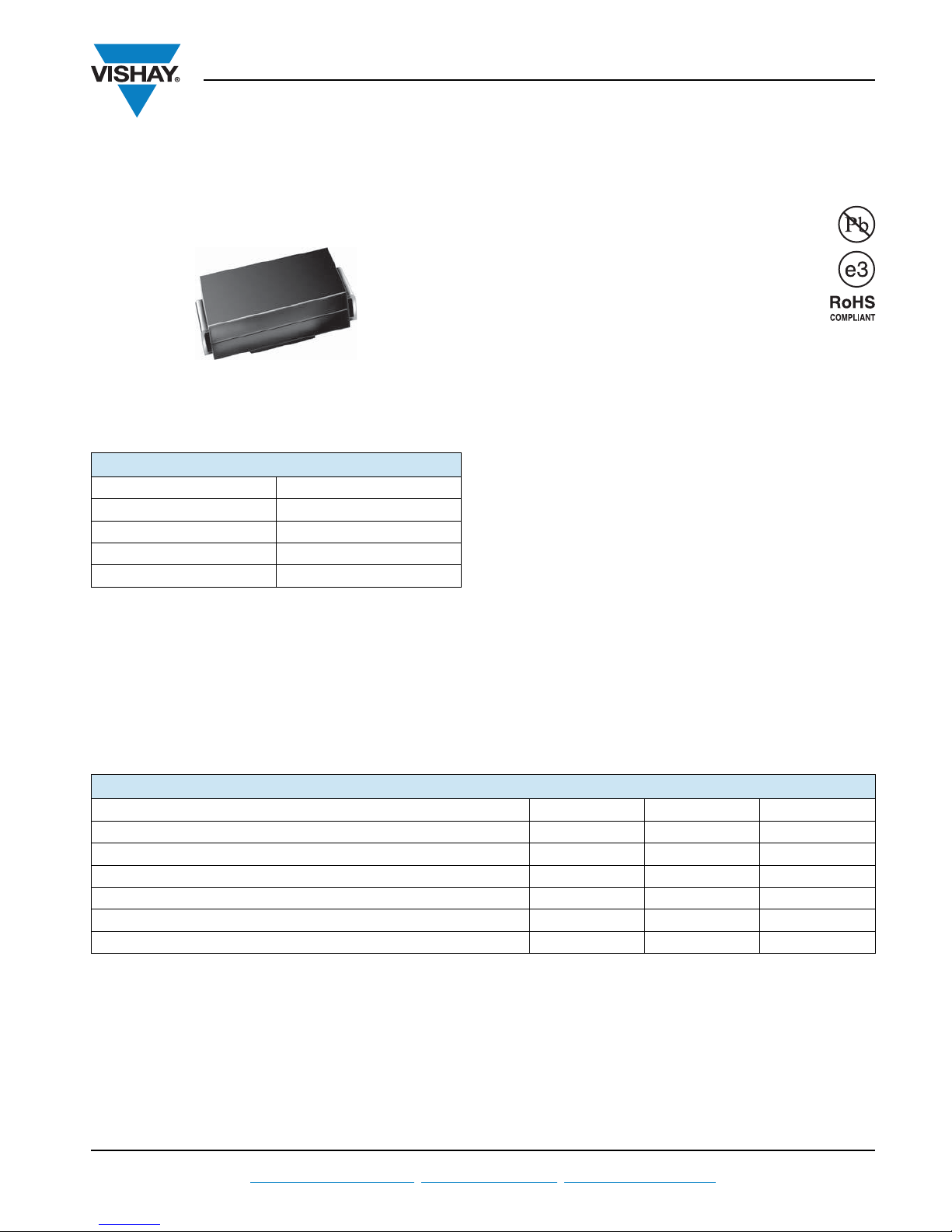
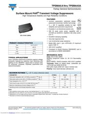
TPSMA6.8 thru TPSMA43A
Vishay General Semiconductor
Document Number: 88405
Revision: 09-Feb-11
For technical questions within your region, please contact one of the following:
DiodesAmericas@vishay.com
, DiodesAsia@vishay.com, DiodesEurope@vishay.com
www.vishay.com
1
Surface Mount PAR
®
Transient Voltage Suppressors
High Temperature Stability and High Reliability Conditions
TYPICAL APPLICATIONS
Use in sensitive electronics protection against voltage
transients induced by inductive load switching and
lighting on ICs, MOSFET, signal lines of sensor units
for consumer, computer, industrial, automotive and
telecommunication.
FEATURES
• Junction passivation optimized design
passivated anisotropic rectifier technology
•T
J
= 185 °C capability suitable for high
reliability and automotive requirement
• Available in uni-directional polarity only
• 400 W peak pulse power capability with a
10/1000 µs waveform, repetitive rate (duty cycle):
0.01 %
• Excellent clamping capability
• Very fast response time
• Low incremental surge resistance
• Meets MSL level 1, per J-STD-020, LF maximum
peak of 260 °C
• AEC-Q101 qualified
• Compliant to RoHS Directive 2002/95/EC and in
accordance to WEEE 2002/96/EC
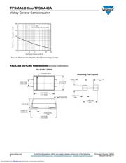
MECHANICAL DATA
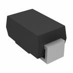
Case: DO-214AC (SMA)
Molding compound meets UL 94 V-0 flammability
rating
Base P/NHE3 - RoHS compliant, AEC-Q101 qualified
Terminals: Matte tin plated leads, solderable per
J-STD-002 and JESD 22-B102
HE3 suffix meets JESD 201 class 2 whisker test
Polarity: Color band denotes cathode end
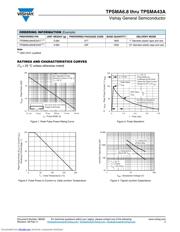
Notes
(1)
Non-repetitive current pulse, per fig. 3 and derated above T
A
= 25 °C per fig. 2
(2)
Mounted on P.C.B. with 0.2" x 0.2" (5.0 mm x 5.0 mm) copper pads attached to each terminal
(3)
Measured on 8.3 ms single half sine-wave or equivalent square wave, duty cycle = 4 pulses per minutes maximum
(4)
Mounted on minimum recommended pad layout
PRIMARY CHARACTERISTICS
V
BR
6.8 V to 43 V
P
PPM
400 W
P
D
1.0 W
I
FSM
40 A
T
J
max. 185 °C
DO-214AC (SMA)
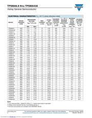
MAXIMUM RATINGS (T
A
= 25 °C unless otherwise noted)
PARAMETER SYMBOL VALUE UNIT
Peak power dissipation with a 10/1000 µs waveform
(1)(2)
(fig. 3) P
PPM
400 W
Peak power pulse current with a 10/1000 µs waveform
(1)
(fig. 1) I
PPM
See next table A
Power dissipation at T
A
= 25 °C
(4)
P
D
1.0 W
Peak forward surge current 8.3 ms single half sine-wave
(3)
I
FSM
40 A
Maximum instantaneous forward voltage at 25 A
(3)
V
F
3.5 V
Operating junction and storage temperature range T
J
, T
STG
- 65 to + 185 °C
Downloaded from Elcodis.com electronic components distributor
器件 Datasheet 文档搜索
AiEMA 数据库涵盖高达 72,405,303 个元件的数据手册,每天更新 5,000 多个 PDF 文件
