Datasheet 搜索 > 模拟开关芯片 > TI(德州仪器) > TS3A5018RGYR 数据手册 > TS3A5018RGYR 数据手册 4/37 页
 器件3D模型
¥ 1.656
TS3A5018RGYR 数据手册 - TI(德州仪器)
制造商:
TI(德州仪器)
分类:
模拟开关芯片
封装:
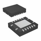
VQFN-16
描述:
TEXAS INSTRUMENTS TS3A5018RGYR 模拟开关, SPDT, 4 放大器, 10 ohm, 2.3V 至 3.6V, VQFN, 16 引脚
Pictures:
3D模型
符号图
焊盘图
引脚图
产品图
页面导航:
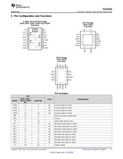
引脚图在P3Hot
典型应用电路图在P18
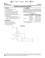
原理图在P1P17P18
封装尺寸在P22P24P25
标记信息在P22P23
封装信息在P21P22P23P24P25
技术参数、封装参数在P4
应用领域在P1P37
电气规格在P5P6P7P8P14
导航目录
TS3A5018RGYR数据手册
Page:
of 37 Go
若手册格式错乱,请下载阅览PDF原文件
TS3A5018
SCDS189G –JANUARY 2005–REVISED MARCH 2015
www.ti.com
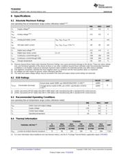
6 Specifications
6.1 Absolute Maximum Ratings
over operating free-air temperature range (unless otherwise noted)
(1)(2)
MIN MAX UNIT
V
+
Supply voltage
(3)
–0.5 4.6 V
V
NC
V
NO
Analog voltage
(3)(4)
–0.5 4.6 V
V
COM
I
K
Analog port diode current V
NC
, V
NO
, V
COM
< 0 –50 mA
I
NC
I
NO
ON-state switch current V
NC
, V
NO
, V
COM
= 0 to 7 V –64 64 mA
I
COM
V
I
Digital input voltage
(3)(4)
–0.5 4.6 V
I
IK
Digital input clamp current V
I
< 0 –50 mA
I
+
Continuous current through V
+
–100 100 mA
I
GND
Continuous current through GND –100 100 mA
T
stg
Storage temperature –65 150 °C
(1) Stresses beyond those listed under Absolute Maximum Ratings may cause permanent damage to the device. These are stress ratings
only, and functional operation of the device at these or any other conditions beyond those indicated under Recommended Operating
Conditions is not implied. Exposure to absolute-maximum-rated conditions for extended periods may affect device reliability.
(2) The algebraic convention, whereby the most negative value is a minimum and the most positive value is a maximum
(3) All voltages are with respect to ground, unless otherwise specified.
(4) The input and output voltage ratings may be exceeded if the input and output clamp-current ratings are observed.
6.2 ESD Ratings
VALUE UNIT
Human-body model (HBM), per ANSI/ESDA/JEDEC JS-001
(1)
±2000
V
(ESD)
Electrostatic discharge V
Charged-device model (CDM), per JEDEC specification JESD22- ±1000
C101
(2)
(1) JEDEC document JEP155 states that 500-V HBM allows safe manufacturing with a standard ESD control process.
(2) JEDEC document JEP157 states that 250-V CDM allows safe manufacturing with a standard ESD control process.
6.3 Recommended Operating Conditions
over operating free-air temperature range (unless otherwise noted)
MIN MAX UNIT
V
I/O
Switch input and output voltage 0 V
+
V
V
+
Supply voltage 1.65 3.6 V
V
I
Control input voltage 0 3.6 V
T
A
Operating temperature -40 85 °C
6.4 Thermal Information
TS3A5018
D DBQ DGV PW RGY RSV
THERMAL METRIC
(1)
UNIT
(SOIC) (SSOP) (TVSOP) (TSSOP) (VQFN) (UQFN)
16 PINS 16 PINS 16 PINS 16 PINS 16 PINS 16 PINS
R
θJA
Junction-to-ambient thermal resistance 73 90 120 108 51 184 °C/W
(1) For more information about traditional and new thermal metrics, see the IC Package Thermal Metrics application report, SPRA953.
4 Submit Documentation Feedback Copyright © 2005–2015, Texas Instruments Incorporated
Product Folder Links: TS3A5018
器件 Datasheet 文档搜索
AiEMA 数据库涵盖高达 72,405,303 个元件的数据手册,每天更新 5,000 多个 PDF 文件
