Datasheet 搜索 > 逻辑控制器 > TI(德州仪器) > TS3DV642A0RUAR 数据手册 > TS3DV642A0RUAR 数据手册 13/32 页

¥ 5.295
TS3DV642A0RUAR 数据手册 - TI(德州仪器)
制造商:
TI(德州仪器)
分类:
逻辑控制器
封装:
WQFN-42
描述:
12通道1 : 2复用器/解复用器with1.8V兼容控制和省电模式 12-Channel 1:2 MUX/DEMUX with1.8V Compatible Control and Power-Down Mode
Pictures:
3D模型
符号图
焊盘图
引脚图
产品图
页面导航:
引脚图在P3P4Hot
典型应用电路图在P14P16P17P18
原理图在P1P13P17P19P21
封装尺寸在P25P27P28
标记信息在P25
封装信息在P24P25P26P27P28
技术参数、封装参数在P5
应用领域在P1P32
电气规格在P6
型号编号列表在P22
导航目录
TS3DV642A0RUAR数据手册
Page:
of 32 Go
若手册格式错乱,请下载阅览PDF原文件
SEL1,
SEL2,
EN
D0+
D0+A
D0+B
CEC_A
CEC_B
CEC
TS3DV642
13
TS3DV642
www.ti.com
SCDS343D –MAY 2013–REVISED DECEMBER 2015
Product Folder Links: TS3DV642
Submit Documentation FeedbackCopyright © 2013–2015, Texas Instruments Incorporated
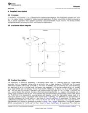
8 Detailed Description
8.1 Overview
TS3DV642 is a 12-channel 1:2 or 2:1 bidirectional multiplexer/demultiplexer. The TS3DV642 operates from a 2.6
to 4.5 V supply, making it suitable for battery-powered applications. It offers low and flat on-state resistance as
well as low I/O capacitance which allows it to achieve a typical bandwidth of up to 7.5 GHz. The device provides
the high bandwidth necessary for HDMI and DisplayPort applications.
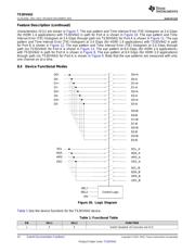
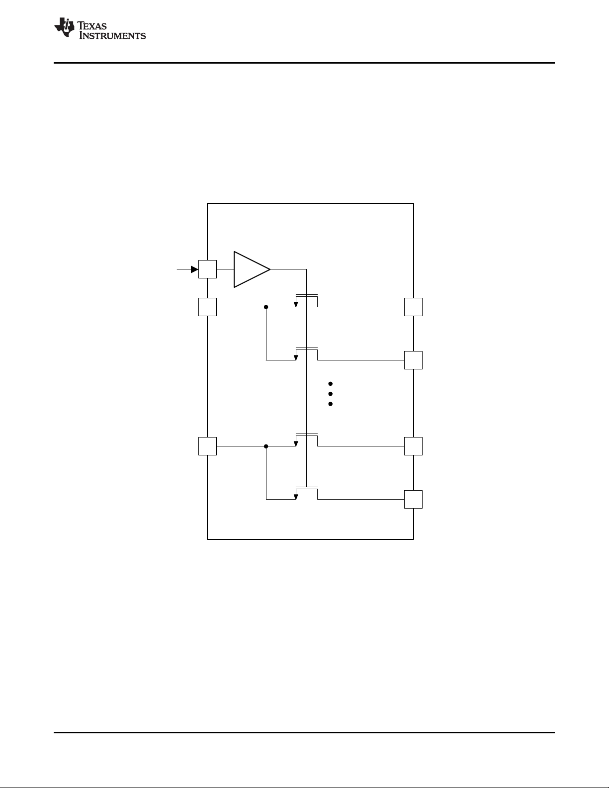
8.2 Functional Block Diagram
8.3 Feature Description
The TS3DV642 is based on proprietary TI technology which uses FET switches driven by a high-voltage
generated from an integrated charge-pump to achieve a low on-state resistance. TS3DV642 has 12-channel
bidirectional switches with a high bandwidth (~ 7.5 GHz). TS3DV642 uses an extremely low power technology
and uses only 50 µA I
CC
in active mode. The device has integrated ESD that can support up to 2-kV Human-
Body Model (HBM) and 1-kV Charge Device Model (CDM). TS3DV642 is offered in a 42-pin QFN package (9
mm x 3.5 mm) with 0.5 mm pitch. The device can support analog I/O signal in 0 to 5 V range. TS3DV642 also
has a special feature that prevents the device from back-powering when the V
CC
supply is not available and an
analog signal is applied on the I/O pin. In this situation this special feature prevents leakage current in the device.
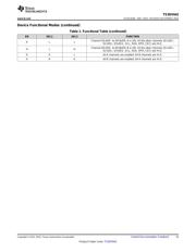
The TS3DV642 is not designed for passing signals with negative swings; the high-speed signals need to be
properly DC biased (usually ~1 V) before being passed to the TS3DV642. The differential S21 characteristics as
a function of frequency for Port A and Port B are shown in Figure 1 and Figure 2, respectively. The figures show
a differential bandwidth of 6.7 GHz and 7.7 GHz for Port A and Port B, respectively. The cross-talk (XTALK)
characteristics as a function of frequency are shown in Figure 3 and Figure 4, respectively. The off-state isolation
(OISO) characteristics for Port A and Port B are shown in Figure 5 and Figure 6, respectively. The return loss
器件 Datasheet 文档搜索
AiEMA 数据库涵盖高达 72,405,303 个元件的数据手册,每天更新 5,000 多个 PDF 文件
