Datasheet 搜索 > 逻辑控制器 > TI(德州仪器) > TS3DV642A0RUAR 数据手册 > TS3DV642A0RUAR 数据手册 6/32 页

¥ 5.295
TS3DV642A0RUAR 数据手册 - TI(德州仪器)
制造商:
TI(德州仪器)
分类:
逻辑控制器
封装:
WQFN-42
描述:
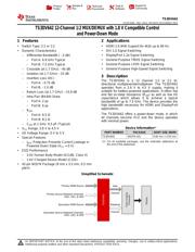
12通道1 : 2复用器/解复用器with1.8V兼容控制和省电模式 12-Channel 1:2 MUX/DEMUX with1.8V Compatible Control and Power-Down Mode
Pictures:
3D模型
符号图
焊盘图
引脚图
产品图
页面导航:
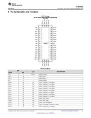
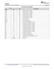
引脚图在P3P4Hot
典型应用电路图在P14P16P17P18
原理图在P1P13P17P19P21
封装尺寸在P25P27P28
标记信息在P25
封装信息在P24P25P26P27P28
技术参数、封装参数在P5
应用领域在P1P32
电气规格在P6
型号编号列表在P22

导航目录
TS3DV642A0RUAR数据手册
Page:
of 32 Go
若手册格式错乱,请下载阅览PDF原文件
6
TS3DV642
SCDS343D –MAY 2013–REVISED DECEMBER 2015
www.ti.com
Product Folder Links: TS3DV642
Submit Documentation Feedback Copyright © 2013–2015, Texas Instruments Incorporated
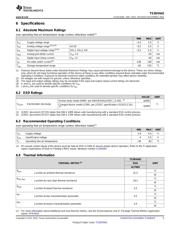
Thermal Information (continued)
THERMAL METRIC
(1)
TS3DV642
UNITRUA
42 PINS
R
θJC(bot)
Junction-to-case (bottom) thermal resistance 2.
°C
W
(1) V
I
, V
O
, I
I
, and I
O
refer to I/O pins, V
IN
refers to the control inputs.
(2) All typical values are at V
CC
= 3.3 V (unless otherwise noted), T
A
= 25°C.
(3) R
ON(FLAT)
is the difference of R
ON
in a given channel at specified voltages.
(4) ΔR
ON
is the difference of RON from center port to any other ports.
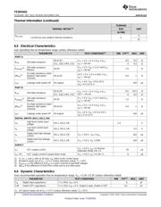
6.5 Electrical Characteristics
over operating free-air temperature range (unless otherwise noted)
PARAMETER TEST CONDITIONS
(1)
MIN TYP
(2)
MAX UNIT
PORT A
R
ON
ON-state resistance
D0 to D3
V
CC
= 3 V, 1.5 V ≤ V
I/O
≤ V
CC
,
I
I/O
= –40 mA
6.5 9.5 Ω
SCL, SDA, HPD, CEC 6 9.5 Ω
R
ON(flat)
(3)
ON-state resistance
flatness
All I/O
V
CC
= 3 V, V
I/O
= 1.5 V and V
CC
,
I
I/O
= –40 mA
1.5 Ω
ΔR
ON
(4)
On-state resistance match
between high-speed
channels
D0 to D3
VCC = 3 V, 1.5 V ≤ VI/O ≤ V
CC
,
I
I/O
= –40 mA
0.4 1 Ω
I
OFF
Leakage under power off All outputs
V
CC
= 0 V, V
I/O
= 0 to 3.6 V,
V
IN
= 0 V to 5.5 V
±10 µA
PORT B
R
ON
ON-state resistance
D0 to D3
V
CC
= 3 V, 1.5 V ≤ V
I/O
≤ V
CC
,
II/O = –40 mA
8.2 10.5 Ω
SCL, SDA, HPD, CEC 6 9.5 Ω
R
ON(flat)
(3)
ON-state resistance
flatness
All I/O
V
CC
= 3 V, V
I/O
= 1.5 V and V
CC
,
I
I/O
= –40 mA
1.5 Ω
ΔR
ON
(4)
On-state resistance match
between high-speed
channels
D0 to D3
V
CC
= 3 V, 1.5 V ≤ V
I/O
≤ V
CC
,
I
I/O
= –40 mA
0.4 1 Ω
I
OFF
Leakage under power off All outputs
V
CC
= 0 V, V
I/O
= 0 V to 3.6 V,
V
IN
= V to 5.5 V
±10 µA
DIGITAL INPUTS (SEL1, SEL2, EN)
V
IH
High-level control input
voltage
SEL1, SEL2, EN 1.4 V
V
IL
Low-level control input
voltage
SEL1, SEL2, EN 0.5 V
I
IH
Digital input high leakage
current
SEL1, SEL2, EN V
CC
= 3.6 V , V
IN
= V
DD
±10 µA
I
IL
Digital input low leakage
current
SEL1, SEL2, EN V
CC
= 3.6 V, V
IN
= GND ±10 µA
SUPPLY
I
CC
VCC supply current
V
CC
= 3.6 V, I
I/O
= 0, Normal
Operation Mode, EN = H
50 µA
I
CC
, PD VCC supply current in power-down mode V
CC
= 3.6 V, I
I/O
= 0, EN = L 6 µA
(1) All Typical Values are at V
CC
= 3.3 V (unless otherwise noted), T
A
= 25°C.
6.6 Dynamic Characteristics
Over recommended operation free-air temperature range, V
CC
= 3.3V ± 0.3V (unless otherwise noted)
PARAMETER TEST CONDITIONS MIN TYP
(1)
MAX UNIT
C
IN
Digital input capacitance f = 1 MHz, V
IN
= 0 V 6 pF
Coff Switch OFF capacitance f = 1 GHz, V
I/O
= 0 V, Output is open, Switch is OFF 0.3 pF
器件 Datasheet 文档搜索
AiEMA 数据库涵盖高达 72,405,303 个元件的数据手册,每天更新 5,000 多个 PDF 文件
