Datasheet 搜索 > TI(德州仪器) > TS3L110 数据手册 > TS3L110 数据手册 4/26 页


¥ 0
TS3L110 数据手册 - TI(德州仪器)
制造商:
TI(德州仪器)
描述:
四路 SPDT 宽频带 10/100 Base-T 局域网开关差动 8 到 4 多路复用器/多路解复用器
Pictures:
3D模型
符号图
焊盘图
引脚图
产品图
页面导航:
导航目录
TS3L110数据手册
Page:
of 26 Go
若手册格式错乱,请下载阅览PDF原文件
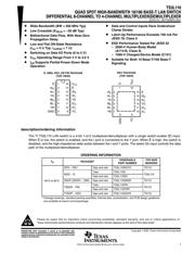
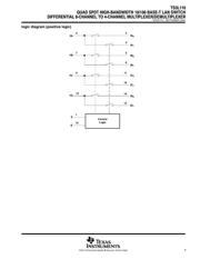
TS3L110
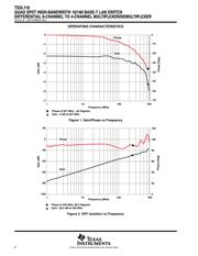
QUAD SPDT HIGH-BANDWIDTH 10/100 BASE-T LAN SWITCH
DIFFERENTIAL 8-CHANNEL TO 4-CHANNEL MULTIPLEXER/DEMULTIPLEXER
SCDS176 − SEPTEMBER 2004
4
POST OFFICE BOX 655303 • DALLAS, TEXAS 75265
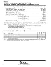
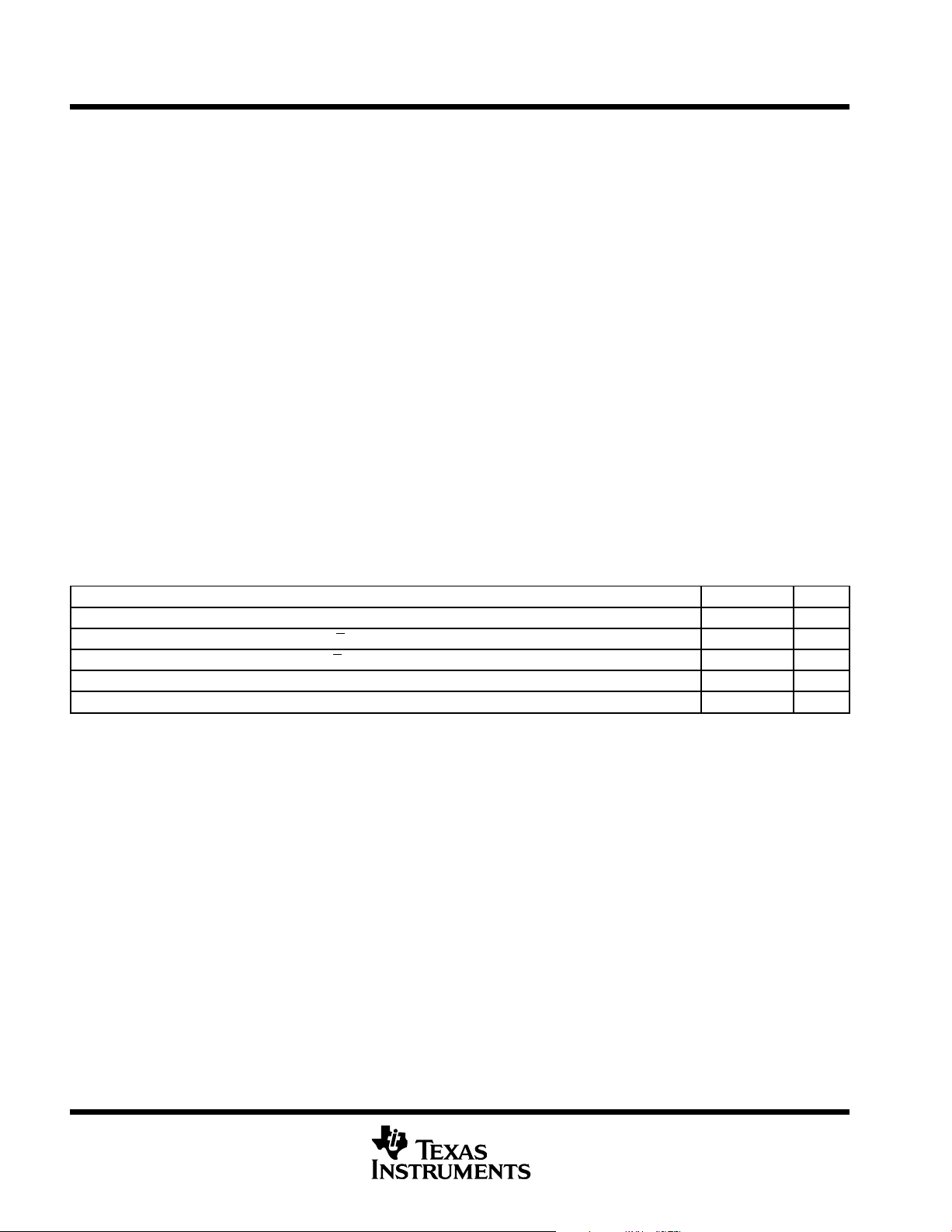
absolute maximum ratings over operating free-air temperature range (unless otherwise noted)
†
Supply voltage range, V
CC
−0.5 V to 4.6 V. . . . . . . . . . . . . . . . . . . . . . . . . . . . . . . . . . . . . . . . . . . . . . . . . . . . . . . . .
Control input voltage range, V
IN
(see Notes 1 and 2) −0.5 V to 7 V. . . . . . . . . . . . . . . . . . . . . . . . . . . . . . . . . . .
Switch I/O voltage range, V
I/O
(see Notes 1, 2, and 3) −0.5 V to 7 V. . . . . . . . . . . . . . . . . . . . . . . . . . . . . . . . . .
Control input clamp current, I
IK
(V
IN
< 0) −50 mA. . . . . . . . . . . . . . . . . . . . . . . . . . . . . . . . . . . . . . . . . . . . . . . . . . .
I/O port clamp current, I
I/OK
(V
I/O
< 0) −50 mA. . . . . . . . . . . . . . . . . . . . . . . . . . . . . . . . . . . . . . . . . . . . . . . . . . . . . .
ON-state switch current, I
I/O
(see Note 4) ±128 mA. . . . . . . . . . . . . . . . . . . . . . . . . . . . . . . . . . . . . . . . . . . . . . . . .
Continuous current through V
CC
or GND terminals ±100 mA. . . . . . . . . . . . . . . . . . . . . . . . . . . . . . . . . . . . . . . . .
Package thermal impedance, θ
JA
(see Note 5): D package 73°C/W. . . . . . . . . . . . . . . . . . . . . . . . . . . . . . . . . . .
(see Note 5): DBQ package 90°C/W. . . . . . . . . . . . . . . . . . . . . . . . . . . . . . . .
(see Note 5): DGV package 120°C/W. . . . . . . . . . . . . . . . . . . . . . . . . . . . . . .
(see Note 5): PW package 108°C/W. . . . . . . . . . . . . . . . . . . . . . . . . . . . . . . .
(see Note 6): RGY package 39°C/W. . . . . . . . . . . . . . . . . . . . . . . . . . . . . . . .
Storage temperature range, T
stg
−65°C to 150°C. . . . . . . . . . . . . . . . . . . . . . . . . . . . . . . . . . . . . . . . . . . . . . . . . . .
†
Stresses beyond those listed under “absolute maximum ratings” may cause permanent damage to the device. These are stress ratings only, and
functional operation of the device at these or any other conditions beyond those indicated under “recommended operating conditions” is not
implied. Exposure to absolute-maximum-rated conditions for extended periods may affect device reliability.
NOTES: 1. All voltages are with respect to ground, unless otherwise specified.
2. The input and output voltage ratings may be exceeded if the input and output clamp-current ratings are observed.
3. V
I
and V
O
are used to denote specific conditions for V
I/O
.
4. I
I
and I
O
are used to denote specific conditions for I
I/O
.
5. The package thermal impedance is calculated in accordance with JESD 51-7.
6. The package thermal impedance is calculated in accordance with JESD 51-5.
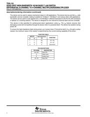
recommended operating conditions (see Note 7)
MIN MAX UNIT
V
CC
Supply voltage 3 3.6 V
V
IH
High-level control input voltage (E, S) 2 5.5 V
V
IL
Low-level control input voltage (E, S) 0 0.8 V
V
I/O
Input/output voltage 0 5.5 V
T
A
Operating free-air temperature −40 85 °C
NOTE 7: All unused control inputs of the device must be held at V
CC
or GND to ensure proper device operation. Refer to the TI application report,
Implications of Slow or Floating CMOS Inputs, literature number SCBA004.
器件 Datasheet 文档搜索
AiEMA 数据库涵盖高达 72,405,303 个元件的数据手册,每天更新 5,000 多个 PDF 文件
