Datasheet 搜索 > USB芯片 > TI(德州仪器) > TS3USB221DRCR 数据手册 > TS3USB221DRCR 数据手册 1/27 页
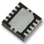
 器件3D模型
¥ 1.927
TS3USB221DRCR 数据手册 - TI(德州仪器)
制造商:
TI(德州仪器)
分类:
USB芯片
封装:
VSON-10
描述:
TEXAS INSTRUMENTS TS3USB221DRCR 接口, USB, 多路复用器/信号分离器开关, USB 2.0, 2.3 V, 3.6 V, SON, 10 引脚
Pictures:
3D模型
符号图
焊盘图
引脚图
产品图
页面导航:
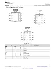
引脚图在P3Hot
典型应用电路图在P13P14
原理图在P1P12P13
封装尺寸在P18P20P21
标记信息在P18
封装信息在P17P18P19P20P21
技术参数、封装参数在P4
应用领域在P1P27
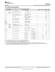
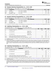
电气规格在P5P6
导航目录
TS3USB221DRCR数据手册
Page:
of 27 Go
若手册格式错乱,请下载阅览PDF原文件
A
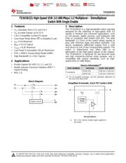
EN (see Note A)
B
Charge
Pump
V
CC
D−
D+
1D−
1D+
2D−
2D+
S
OE
Digital Control
Product
Folder
Sample &
Buy
Technical
Documents
Tools &
Software
Support &
Community
TS3USB221
SCDS220H –NOVEMBER 2006–REVISED MARCH 2015
TS3USB221 High-Speed USB 2.0 (480-Mbps) 1:2 Multiplexer – Demultiplexer
Switch With Single Enable
1 Features 3 Description
The TS3USB221 is a high-bandwidth switch specially
1
• V
CC
Operation from 2.3 V and 3.6 V
designed for the switching of high-speed USB 2.0
• V
I/O
Accepts Signals up to 5.5 V
signals in handset and consumer applications, such
• 1.8-V Compatible Control-Pin Inputs
as cell phones, digital cameras, and notebooks with
hubs or controllers with limited USB I/Os. The wide
• Low-Power Mode When OE Is Disabled (1 μA)
bandwidth (1.1 GHz) of this switch allows signals to
• r
ON
= 6 Ω Maximum
pass with minimum edge and phase distortion. The
• Δr
ON
= 0.2 Ω Typical
device multiplexes differential outputs from a USB
host device to one of two corresponding outputs. The
• C
io(on)
= 6 pF Maximum
switch is bidirectional and offers little or no
• Low Power Consumption (30 μA Maximum)
attenuation of the high-speed signals at the outputs.
• ESD > 2000-V Human-Body Model (HBM)
The TS3USB221 is designed for low bit-to-bit skew
• High Bandwidth (1.1 GHz Typical)
and high channel-to-channel noise isolation, and is
compatible with various standards, such as high-
speed USB 2.0 (480 Mbps).
2 Applications
• Routes Signals for USB 1.0, 1.1, and 2.0
Device Information
(1)
• Mobile Industry Processor Interface (MIPI™)
PART NUMBER PACKAGE BODY SIZE (NOM)
Signal Routing
VSON (10) 3.00 mm × 3.00 mm
TS3USB221
• MHL 1.0
UQFN (10) 1.50 mm × 2.00 mm
(1) For all available packages, see the orderable addendum at
the end of the data sheet.
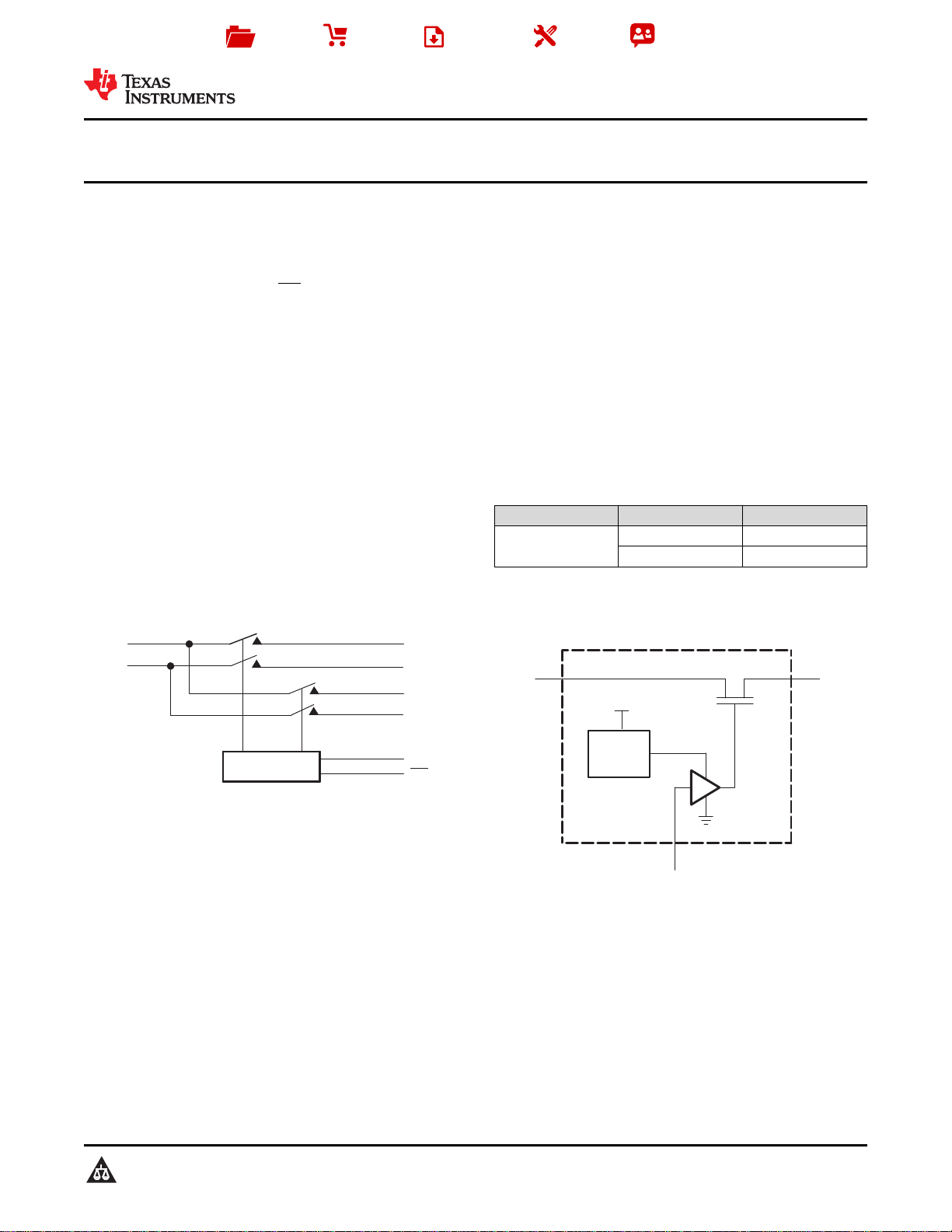
Block Diagram
Simplified Schematic, Each FET Switch (SW)
A. EN is the internal enable signal applied to
the switch.
1
An IMPORTANT NOTICE at the end of this data sheet addresses availability, warranty, changes, use in safety-critical applications,
intellectual property matters and other important disclaimers. PRODUCTION DATA.
器件 Datasheet 文档搜索
AiEMA 数据库涵盖高达 72,405,303 个元件的数据手册,每天更新 5,000 多个 PDF 文件
