Datasheet 搜索 > 可编程定时器芯片 > ST Microelectronics(意法半导体) > TS556CD 数据手册 > TS556CD 数据手册 3/19 页
 器件3D模型
¥ 2.738
TS556CD 数据手册 - ST Microelectronics(意法半导体)
制造商:
ST Microelectronics(意法半导体)
分类:
可编程定时器芯片
封装:
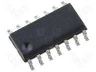
SOIC-14
描述:
低功率双路CMOS定时器 LOW POWER DUAL CMOS TIMERS
Pictures:
3D模型
符号图
焊盘图
引脚图
产品图
页面导航:
引脚图在P1Hot
原理图在P4P5
封装尺寸在P15P16
型号编码规则在P17
标记信息在P17
封装信息在P17
技术参数、封装参数在P3
应用领域在P13P14
电气规格在P6P7P8P9P10P11P12

导航目录
TS556CD数据手册
Page:
of 19 Go
若手册格式错乱,请下载阅览PDF原文件
DocID4078 Rev 3 3/19
TS556 Absolute maximum ratings and operating conditions
19
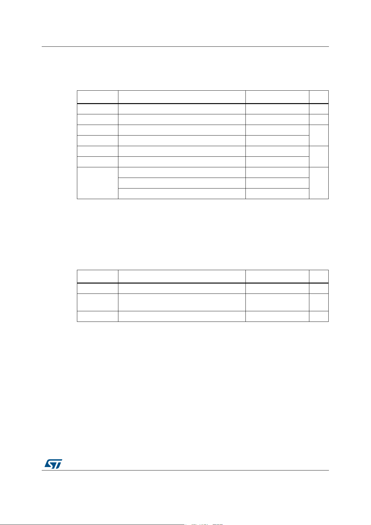
1 Absolute maximum ratings and operating conditions
Table 1. Absolute maximum ratings
Symbol Parameter Value Unit
V
CC
Supply voltage 18 V
I
OUT
Output current ± 100 mA
R
thja
Thermal resistance junction to ambient
(1)
1. Short-circuits can cause excessive heating. These values are typical and specified for a four layers PCB.
105
°C/W
R
thjc
Thermal resistance junction to case
(1)
31
T
j
Junction Temperature 150
°C
T
stg
Storage Temperature Range -65 to 150
ESD
Human body model (HBM)
(2)
2. Human body model: a 100 pF capacitor is charged to the specified voltage, then discharged through a
1.5kΩ resistor between two pins of the device. This is done for all couples of connected pin combinations
while the other pins are floating.
1200
VMachine model (MM)
(3)
3. Machine model: a 200 pF capacitor is charged to the specified voltage, then discharged directly between
two pins of the device with no external series resistor (internal resistor < 5 Ω). This is done for all couples of
connected pin combinations while the other pins remain floating.
200
Charged device model (CDM)
(4)
4. Charged device model: all pins plus package are charged together to the specified voltage and then
discharged directly to the ground.
1000
Table 2. Operating conditions
Symbol Parameter Value Unit
V
CC
Supply voltage 2 to 16 V
I
OUT
Output sink current
Output source current
10
50
mA
T
oper
Operating free air temperature range -40 to 125 °C
器件 Datasheet 文档搜索
AiEMA 数据库涵盖高达 72,405,303 个元件的数据手册,每天更新 5,000 多个 PDF 文件
