Datasheet 搜索 > 电压电平转换器 > TI(德州仪器) > TXB0104QPWRQ1 数据手册 > TXB0104QPWRQ1 数据手册 2/20 页

 器件3D模型
¥ 1.714
TXB0104QPWRQ1 数据手册 - TI(德州仪器)
制造商:
TI(德州仪器)
分类:
电压电平转换器
封装:
TSSOP-14
描述:
TEXAS INSTRUMENTS TXB0104QPWRQ1 芯片, 电平转换器, 双向, 4位, TSSOP-14
Pictures:
3D模型
符号图
焊盘图
引脚图
产品图
页面导航:
封装尺寸在P12P13P14
封装信息在P12P13P14
应用领域在P20
导航目录
TXB0104QPWRQ1数据手册
Page:
of 20 Go
若手册格式错乱,请下载阅览PDF原文件
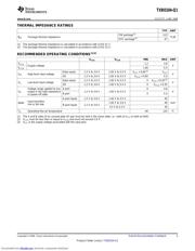
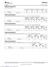
ABSOLUTE MAXIMUM RATINGS
(1)
TXB0104-Q1
SCES727 – JUNE 2008 ......................................................................................................................................................................................................
www.ti.com
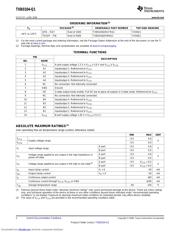
ORDERING INFORMATION
(1)
T
A
PACKAGE
(2)
ORDERABLE PART NUMBER TOP-SIDE MARKING
QFN – RGY Reel of 1000 TXB0104QRGYRQ1 YE04Q1
– 40 ° C to 125 ° C
TSSOP – PW Reel of 2000 TXB0104QPWRQ1 YE04Q1
(1) For the most current package and ordering information, see the Package Option Addendum at the end of this document, or see the TI
web site at www.ti.com .
(2) Package drawings, thermal data, and symbolization are available at www.ti.com/packaging .
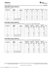
TERMINAL FUNCTIONS
PIN
DESCRIPTION
NO. NAME
1 V
CCA
A-port supply voltage 1.2 V ≤ V
CCA
≤ 3.6 V and V
CCA
≤ V
CCB
.
2 A1 Input/output 1. Referenced to V
CCA
.
3 A2 Input/output 2. Referenced to V
CCA
.
4 A3 Input/output 3. Referenced to V
CCA
.
5 A4 Input/output 4. Referenced to V
CCA
.
6 NC No connection. Not internally connected.
7 GND Ground
8 OE 3-state output-mode enable. Pull OE low to place all outputs in 3-state mode. Referenced to V
CCA
.
9 NC No connection. Not internally connected.
10 B4 Input/output 4. Referenced to V
CCB
.
11 B3 Input/output 3. Referenced to V
CCB
.
12 B2 Input/output 2. Referenced to V
CCB
.
13 B1 Input/output 1. Referenced to V
CCB
.
14 V
CCB
B-port supply voltage 1.65 V ≤ V
CCB
≤ 5.5 V.
over operating free-air temperature range (unless otherwise noted)
MIN MAX UNIT
V
CCA
– 0.5 4.6
Supply voltage range V
V
CCB
– 0.5 6.5
A port – 0.5 4.6
V
I
Input voltage range V
B port – 0.5 6.5
A port – 0.5 4.6
Voltage range applied to any output in the high-impedance or
V
O
V
power-off state
B port -0.5 6.5
A port – 0.5 V
CCA
+ 0.5
V
O
Voltage range applied to any output in the high or low state
(2)
V
B port – 0.5 V
CCB
+ 0.5
I
IK
Input clamp current V
I
< 0 – 50 mA
I
OK
Output clamp current V
O
< 0 – 50 mA
I
O
Continuous output current ± 50 mA
Continuous current through V
CCA
, V
CCB
, or GND ± 100 mA
T
stg
Storage temperature range – 65 150 ° C
(1) Stresses beyond those listed under " absolute maximum ratings " may cause permanent damage to the device. These are stress ratings
only, and functional operation of the device at these or any other conditions beyond those indicated under " recommended operating
conditions " is not implied. Exposure to absolute-maximum-rated conditions for extended periods may affect device reliability.
(2) The value of V
CCA
and V
CCB
are provided in the recommended operating conditions table.
2 Submit Documentation Feedback Copyright © 2008, Texas Instruments Incorporated
Product Folder Link(s): TXB0104-Q1
Downloaded from Elcodis.com electronic components distributor
器件 Datasheet 文档搜索
AiEMA 数据库涵盖高达 72,405,303 个元件的数据手册,每天更新 5,000 多个 PDF 文件
