Datasheet 搜索 > 开发套件 > TI(德州仪器) > TXB0304EVM 数据手册 > TXB0304EVM 数据手册 1/25 页

¥ 32.168
TXB0304EVM 数据手册 - TI(德州仪器)
制造商:
TI(德州仪器)
分类:
开发套件
描述:
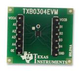
TEXAS INSTRUMENTS TXB0304EVM 评估模块, TXB0304, 4位自动方向感应, 双向电压转换器
Pictures:
3D模型
符号图
焊盘图
引脚图
产品图
页面导航:
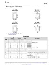
引脚图在P3Hot
典型应用电路图在P1P13
原理图在P1P10P13
封装尺寸在P17P19P20
标记信息在P17
封装信息在P16P17P18P19P20
技术参数、封装参数在P4
应用领域在P1P25
电气规格在P5
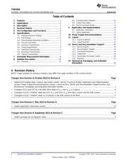
导航目录
TXB0304EVM数据手册
Page:
of 25 Go
若手册格式错乱,请下载阅览PDF原文件
Processor Peripheral
V
CCA
V
CCB
Product
Folder
Sample &
Buy
Technical
Documents
Tools &
Software
Support &
Community
TXB0304
SCES831E –SEPTEMBER 2011–REVISED NOVEMEBER 2015
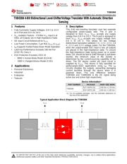
TXB0304 4-Bit Bidirectional Level-Shifter/Voltage Translator With Automatic Direction
Sensing
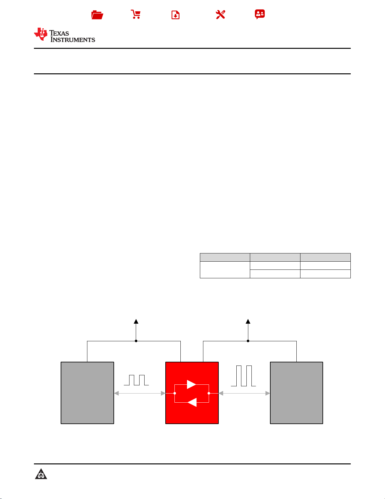
1 Features 3 Description
This 4-bit non-inverting translator uses two separate
1
• Fully Symmetric Supply Voltages, 0.9 V to 3.6 V
configurable power-supply rails. The A port is
on A Port and 0.9 V to 3.6 V
designed to track V
CCA
. V
CCA
accepts any supply
• V
CC
Isolation Feature – If Either V
CC
Input is at
voltage from 0.9 V to 3.6 V. The B port is designed to
GND, all Outputs are in High-Impedance State
track V
CCB
. V
CCB
accepts any supply voltage from
0.9 V to 3.6 V. This allows for low Voltage
• OE Input Circuit Referenced to V
CCA
bidirectional translation between 1 V, 1.2 V, 1.5 V, 1.8
• Low Power Consumption, 5 μA Max (I
CCA
or I
CCB
)
V, 2.5 V and 3.3 V voltage nodes. For the TXB0304,
• I
off
Supports Partial-Power-Down Mode Operation
when the output-enable (OE) input is low, all outputs
• Latch-Up Performance Exceeds 100 mA Per
are placed in the high-impedance state. To ensure
JESD 78, Class II the high-impedance state during power up or power
down, OE should be tied to GND through a pull-down
• ESD Protection Exceeds JESD 22
resistor; the minimum value of the resistor is
– 8000 V Human-Body Model (A114-B)
determined by the current-sourcing capability of the
– 1000 V Charged-Device Model (C101)
driver. The OE device control pin input circuit is
supplied by V
CCA
. This device is fully specified for
partial-power-down applications using I
off
. The I
off
2 Applications
circuitry disables the outputs, preventing damaging
• Personal Electronics
current backflow through the device when it is
• Industrial
powered down. The only difference between
TXB0304 and TXBN0304 is the OE signal being
• Enterprise
active low and active high respectively.
• Telecom
Device Information
(1)
PART NUMBER PACKAGE BODY SIZE (NOM)
RUT UQFN (12) 2.00 mm × 1.70 mm
TXB0304
RSV UQFN (16) 2.60 mm × 1.80 mm
(1) For all available packages, see the orderable addendum at
the end of the datasheet.
Typical Application Block Diagram for TXB0304
1
An IMPORTANT NOTICE at the end of this data sheet addresses availability, warranty, changes, use in safety-critical applications,
intellectual property matters and other important disclaimers. PRODUCTION DATA.
器件 Datasheet 文档搜索
AiEMA 数据库涵盖高达 72,405,303 个元件的数据手册,每天更新 5,000 多个 PDF 文件
