Datasheet 搜索 > 电压电平转换器 > TI(德州仪器) > TXS0102DQER 数据手册 > TXS0102DQER 数据手册 1/35 页

¥ 1.115
TXS0102DQER 数据手册 - TI(德州仪器)
制造商:
TI(德州仪器)
分类:
电压电平转换器
封装:
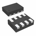
XFDFN-8
描述:
TEXAS INSTRUMENTS TXS0102DQER 芯片, 电平转换器, 2位, X2SON-8
Pictures:
3D模型
符号图
焊盘图
引脚图
产品图
页面导航:
引脚图在P3Hot
典型应用电路图在P1P16
原理图在P1P13
封装尺寸在P20P22P23P30
焊盘布局在P31
标记信息在P20P21
封装信息在P19P20P21P22P23
技术参数、封装参数在P4
应用领域在P1
电气规格在P6


导航目录
TXS0102DQER数据手册
Page:
of 35 Go
若手册格式错乱,请下载阅览PDF原文件
Product
Folder
Sample &
Buy
Technical
Documents
Tools &
Software
Support &
Community
An IMPORTANT NOTICE at the end of this data sheet addresses availability, warranty, changes, use in safety-critical applications,
intellectual property matters and other important disclaimers. PRODUCTION DATA.
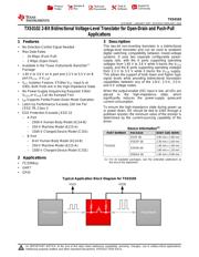
TXS0102
SCES640F –JANUARY 2007–REVISED FEBRUARY 2016
TXS0102 2-Bit Bidirectional Voltage-Level Translator for Open-Drain and Push-Pull
Applications
1
1 Features
1
• No Direction-Control Signal Needed
• Max Data Rates
– 24 Mbps (Push Pull)
– 2 Mbps (Open Drain)
• Available in the Texas Instruments NanoStar™
Package
• 1.65 V to 3.6 V on A port and 2.3 V to 5.5 V on B
port (V
CCA
≤ V
CCB
)
• V
CC
Isolation Feature: If Either V
CC
Input Is at
GND, Both Ports Are in the High-Impedance State
• No Power-Supply Sequencing Required: Either
V
CCA
or V
CCB
Can Be Ramped First
• I
off
Supports Partial-Power-Down Mode Operation
• Latch-Up Performance Exceeds 100 mA Per
JESD 78, Class II
• ESD Protection Exceeds JESD 22
– A Port
– 2500-V Human-Body Model (A114-B)
– 250-V Machine Model (A115-A)
– 1500-V Charged-Device Model (C101)
– B Port
– 8-kV Human-Body Model (A114-B)
– 250-V Machine Model (A115-A)
– 1500-V Charged-Device Model (C101)
2 Applications
• I
2
C/SMBus
• UART
• GPIO
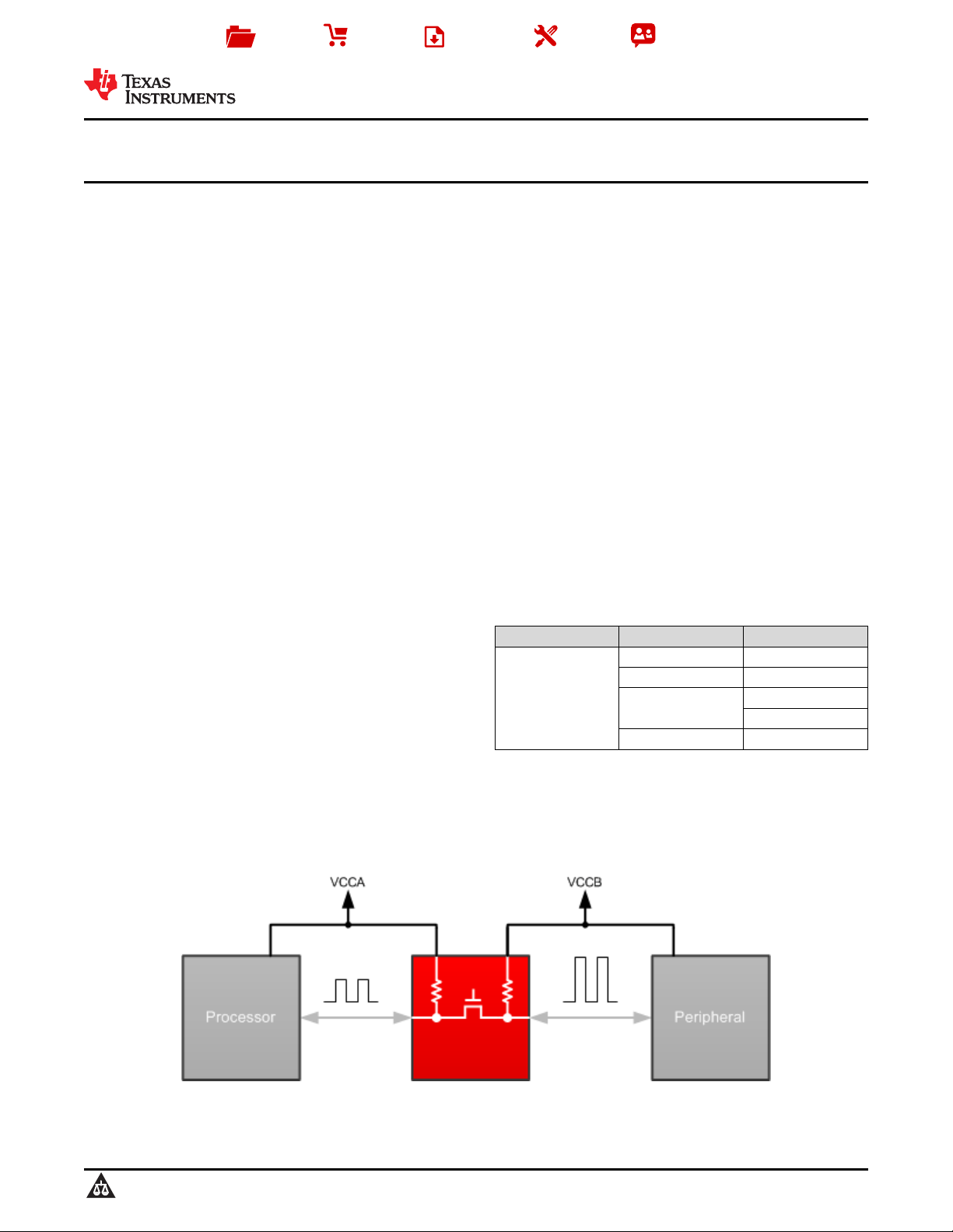
3 Description
This two-bit non-inverting translator is a bidirectional
voltage-level translator and can be used to establish
digital switching compatibility between mixed-voltage
systems. It uses two separate configurable power-
supply rails, with the A ports supporting operating
voltages from 1.65 V to 3.6 V while it tracks the V
CCA
supply, and the B ports supporting operating voltages
from 2.3 V to 5.5 V while it tracks the V
CCB
supply.
This allows the support of both lower and higher logic
signal levels while providing bidirectional translation
capabilities between any of the 1.8-V, 2.5-V, 3.3-V,
and 5-V voltage nodes.
When the output-enable (OE) input is low, all I/Os are
placed in the high-impedance state, which
significantly reduces the power-supply quiescent
current consumption.
To ensure the high-impedance state during power up
or power down, OE should be tied to GND through a
pulldown resistor; the minimum value of the resistor is
determined by the current-sourcing capability of the
driver.
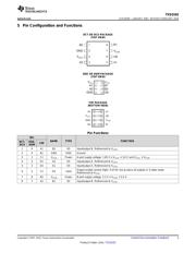
Device Information
(1)
PART NUMBER PACKAGE BODY SIZE (NOM)
TXS0102
SSOP (8) 2.95 mm x 2.80 mm
VSSOP (8) 2.30 mm x 2.00 mm
X2SON (8)
1.40 mm x 1.00 mm
1.80 mm x 1.20 mm
DSBGA (8) 1.90 mm x 0.90 mm
(1) For all available packages, see the orderable addendum at
the end of the datasheet.
Typical Application Block Diagram for TXS010X
器件 Datasheet 文档搜索
AiEMA 数据库涵盖高达 72,405,303 个元件的数据手册,每天更新 5,000 多个 PDF 文件
