Datasheet 搜索 > 电压电平转换器 > TI(德州仪器) > TXS0104EYZTR 数据手册 > TXS0104EYZTR 数据手册 16/33 页
 器件3D模型
¥ 0.698
TXS0104EYZTR 数据手册 - TI(德州仪器)
制造商:
TI(德州仪器)
分类:
电压电平转换器
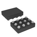
封装:
DSBGA-12
描述:
4位双向电压电平转换为漏极开路和推挽应用 4-BIT BIDIRECTIONAL VOLTAGE-LEVEL TRANSLATOR FOR OPEN-DRAIN AND PUSH-PULL APPLICATIONS
Pictures:
3D模型
符号图
焊盘图
引脚图
产品图
页面导航:
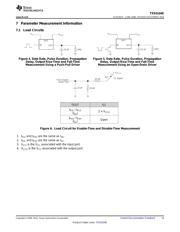
引脚图在P3P4Hot
典型应用电路图在P17
原理图在P15P17
封装尺寸在P21P23P24
标记信息在P21P22
封装信息在P20P21P22P23P24
技术参数、封装参数在P5
应用领域在P1
电气规格在P7
导航目录
TXS0104EYZTR数据手册
Page:
of 33 Go
若手册格式错乱,请下载阅览PDF原文件
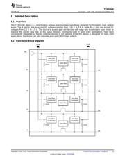
V
CCA
A
B
10 kΩ
10 kΩ
T2
T1
V
CCB
One-shot One-shot
Gate Bias
TXS0104E
SCES651F –JUNE 2006–REVISED DECEMBER 2014
www.ti.com
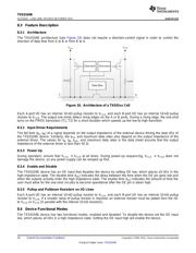
8.3 Feature Description
8.3.1 Architecture
The TXS0104E architecture (see Figure 10) does not require a direction-control signal in order to control the
direction of data flow from A to B or from B to A.
Figure 10. Architecture of a TXS01xx Cell
Each A-port I/O has an internal 10-kΩ pullup resistor to V
CCA
, and each B-port I/O has an internal 10-kΩ pullup
resistor to V
CCB
. The output one-shots detect rising edges on the A or B ports. During a rising edge, the one-shot
turns on the PMOS transistors (T1, T2) for a short duration which speeds up the low-to-high transition.
8.3.2 Input Driver Requirements
The fall time (t
fA
, t
fB
) of a signal depends on the output impedance of the external device driving the data I/Os of
the TXS0104E device. Similarly, the t
PHL
and maximum data rates also depend on the output impedance of the
external driver. The values for t
fA
, t
fB
, t
PHL
, and maximum data rates in the data sheet assume that the output
impedance of the external driver is less than 50 Ω.
8.3.3 Power Up
During operation, ensure that V
CCA
≤ V
CCB
at all times. During power-up sequencing, V
CCA
≥ V
CCB
does not
damage the device, so any power supply can be ramped up first.
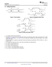
8.3.4 Enable and Disable
The TXS0104E device has an OE input that disables the device by setting OE low, which places all I/Os in the
high-impedance state. The disable time (t
dis
) indicates the delay between the time when the OE pin goes low and
when the outputs actually enter the high-impedance state. The enable time (t
en
) indicates the amount of time the
user must allow for the one-shot circuitry to become operational after the OE pin is taken high.
8.3.5 Pullup and Pulldown Resistors on I/O Lines
Each A-port I/O has an internal 10-kΩ pullup resistor to V
CCA
, and each B-port I/O has an internal 10-kΩ pullup
resistor to V
CCB
. If a smaller value of pullup resistor is required, an external resistor must be added from the I/O
to V
CCA
or V
CCB
(in parallel with the internal 10-kΩ resistors).
8.4 Device Functional Modes
The TXS0104E device has two functional modes, enabled and disabled. To disable the device set the OE input
low, which places all I/Os in a high impedance state. Setting the OE input high will enable the device.
16 Submit Documentation Feedback Copyright © 2006–2014, Texas Instruments Incorporated
Product Folder Links: TXS0104E
器件 Datasheet 文档搜索
AiEMA 数据库涵盖高达 72,405,303 个元件的数据手册,每天更新 5,000 多个 PDF 文件
