Datasheet 搜索 > 稳压芯片 > TI(德州仪器) > UC2524DWG4 数据手册 > UC2524DWG4 数据手册 6/16 页
 器件3D模型
¥ 0
UC2524DWG4 数据手册 - TI(德州仪器)
制造商:
TI(德州仪器)
分类:
稳压芯片
封装:
SOIC-16
描述:
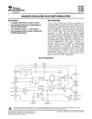
高级稳压脉宽调制器 ADVANCED REGULATING PULSE WIDTH MODULATORS
Pictures:
3D模型
符号图
焊盘图
引脚图
产品图
页面导航:
导航目录
UC2524DWG4数据手册
Page:
of 16 Go
若手册格式错乱,请下载阅览PDF原文件
www.ti.com
APPLICATION INFORMATION
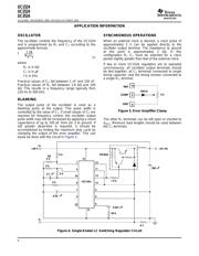
OSCILLATOR SYNCHRONOUS OPERATIONS
f
1.18
R
T
C
T
(1)
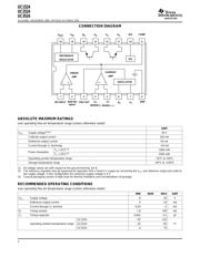
BLANKING
REF
COMP
9
GND
8
1N916
16
5 k
V+
+28 V
V−
1
2
16
6
7
3
10
15
12
11
13
14
4
5
9
9
5 k
R2
5 k
5 k
0.1
mF
5 k
3 k
0.02
mF
500
mF
1.5 k
0.001
mF
50 k
0.1
UC1524
PIC600
+5V, 5A
UC1524
UC2524
UC3524
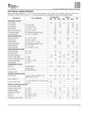
SLUS180E – NOVEMBER 1999 – REVISED OCTOBER 2005
The oscillator controls the frequency of the UC1524 When an external clock is desired, a clock pulse of
and is programmed by R
T
and C
T
according to the approximately 3 V can be applied directly to the
approximate formula: oscillator output terminal. The impedance to ground
at this point is approximately 2 k Ω . In this
configuration R
T
C
T
must be selected for a clock
period slightly greater than that of the external clock.
where
If two or more UC1524 regulators are to operated
R
T
is in k Ω
synchronously, all oscillator output terminals should
be tied together, all C
T
terminals connected to single
C
T
is in µ F
timing capacitor, and the timing resistor connected to
f is in kHz
a single R
T
, terminal.
Practical values of C
T
fall between 1 nF and 100 nF.
Practical values of R
T
fall between 1.8 k Ω and 100
k Ω . This results in a frequency range typically from
120 Hz to 500 kHz.
The output pulse of the oscillator is used as a
blanking pulse at the output. This pulse width is
Figure 5. Error Amplifier Clamp
controlled by the value of C
T
. If small values of C
T
are
required for frequency control, the oscillator output
pulse width may still be increased by applying a shunt
The other R
T
terminals can be left open or shorted to
capacitance of up to 100 pF from pin 3 to ground. If
V
REF
. Minimum lead lengths should be used between
still greater dead-time is required, it should be
the C
T
terminals.
accomplished by limiting the maximum duty cycle by
clamping the output of the error amplifier. This can
easily be done with the circuit in Figure 5 .
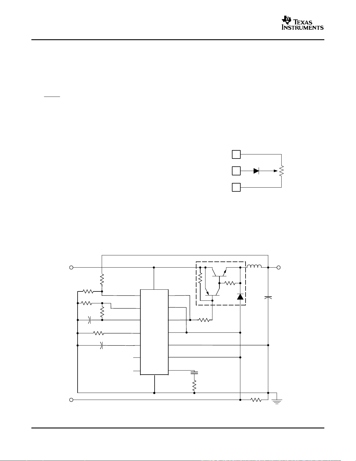
Figure 6. Single-Ended LC Switching Regulator Circuit
6
器件 Datasheet 文档搜索
AiEMA 数据库涵盖高达 72,405,303 个元件的数据手册,每天更新 5,000 多个 PDF 文件
