Datasheet 搜索 > 稳压芯片 > TI(德州仪器) > UC3825AN 数据手册 > UC3825AN 数据手册 3/19 页

 器件3D模型
¥ 46.803
UC3825AN 数据手册 - TI(德州仪器)
制造商:
TI(德州仪器)
分类:
稳压芯片
封装:
PDIP-16
描述:
Texas Instruments隔离式回扫电源控制器提供恒定电压 (CV) 和恒定电流 (CC) 输出调节,用于提高对较大负载阶跃的瞬时响应。 初级侧调节 (PSR) 无需光耦合器。### 回扫控制器,Texas Instruments电流模式和电压模式 PWM 控制器 初级侧调节 峰值功率模式 低功率
Pictures:
3D模型
符号图
焊盘图
引脚图
产品图
页面导航:
引脚图在P2Hot
原理图在P1P11
封装尺寸在P12P13P14P15P17P18
型号编码规则在P2
标记信息在P12P13P14P15P16
封装信息在P12P13P14P15P16P17P18
技术参数、封装参数在P3
应用领域在P16P19
电气规格在P4P5


导航目录
UC3825AN数据手册
Page:
of 19 Go
若手册格式错乱,请下载阅览PDF原文件
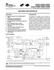
UC1823A, UC2823A, UC2823B,
UC3823A, UC3823B, UC1825A,
UC2825A, UC2825B, UC3825A, UC3825B
SLUS334E − AUGUST 1995 − REVISED SEPTEMBER 2010
www.ti.com
3
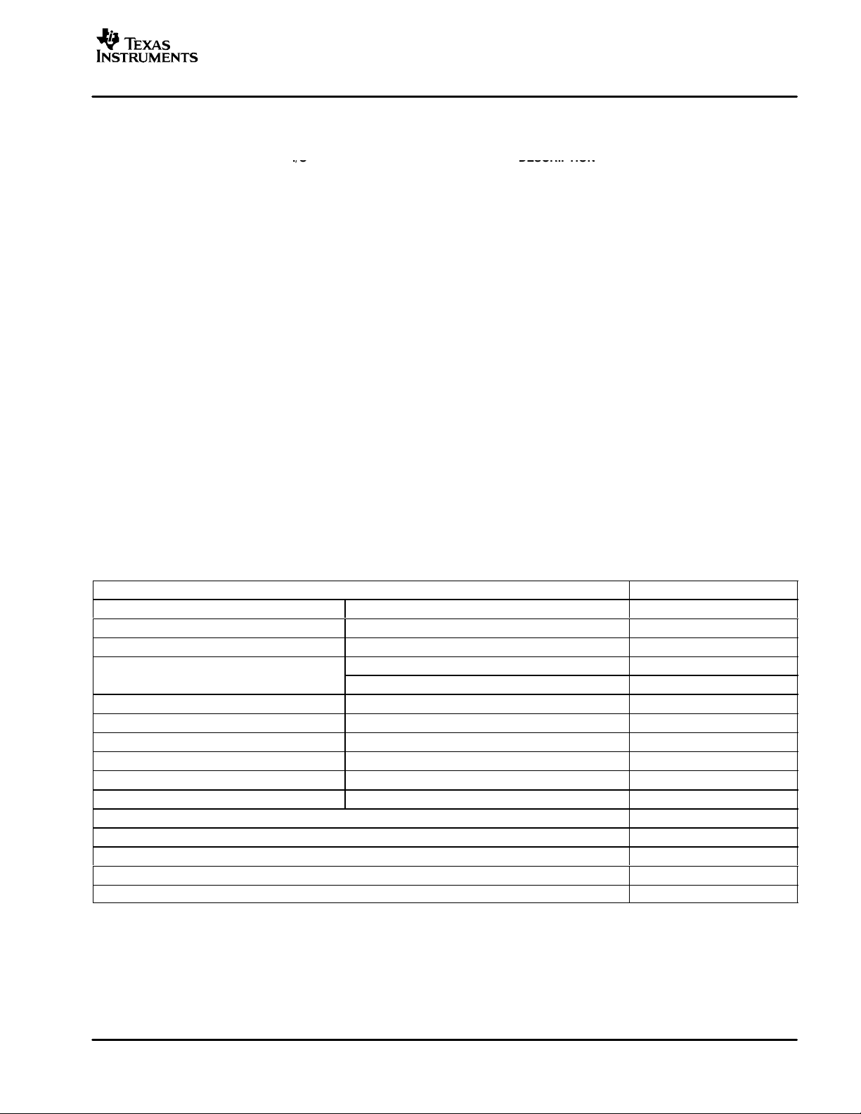
TERMINAL FUNCTIONS
TERMINAL
NAME
NO. I/O DESCRIPTION
NAME
J or DW Q or L
I/O
DESCRIPTION
CLK/LEB 4 5 O Output of the internal oscillator
CT 6 8 I
Timing capacitor connection pin for oscillator frequency programming. The timing capacitor should
be connected to the device ground using minimal trace length.
EAOUT 3 4 O Output of the error amplifier for compensation
GND 10 13 − Analog ground return pin
ILIM 9 12 I Input to the current limit comparator
INV 1 2 I Inverting input to the error amplifier
NI 2 3 I Non-inverting input to the error amplifier
OUTA 11 14 O High current totem pole output A of the on-chip drive stage.
OUTB 14 18 O High current totem pole output B of the on-chip drive stage.
PGND 12 15 − Ground return pin for the output driver stage
RAMP 7 9 I
Non-inverting input to the PWM comparator with 1.25-V internal input offset. In voltage mode
operation, this serves as the input voltage feed-forward function by using the CT ramp. In peak
current mode operation, this serves as the slope compensation input.
RT 5 7 I Timing resistor connection pin for oscillator frequency programming
SS 8 10 I Soft-start input pin which also doubles as the maximum duty cycle clamp.
VC 13 17 −
Power supply pin for the output stage. This pin should be bypassed with a 0.1-μF monolithic ceramic
low ESL capacitor with minimal trace lengths.
VCC 15 19 −
Power supply pin for the device. This pin should be bypassed with a 0.1-μF monolithic ceramic low
ESL capacitor with minimal trace lengths
VREF 16 20 O
5.1-V reference. For stability, the reference should be bypassed with a 0.1-μF monolithic ceramic
low ESL capacitor and minimal trace length to the ground plane.
ABSOLUTE MAXIMUM RATINGS
over operating free-air temperature range unless otherwise noted
(1)
UNIT
V
IN
Supply voltage, VC, VCC 22 V
I
O
Source or sink current, DC OUTA, OUTB 0.5 A
I
O
Source or sink current, pulse (0.5 μs) OUTA, OUTB 2.2 A
Analog inputs
INV, NI, RAMP −0.3 V to 7 V
Analog inputs
ILIM, SS −0.3 V to 6 V
Power ground PGND ±0.2 V
Outputs OUTA, OUTB limits PGND −0.3 V to V
C
+0.3 V
I
CLK
Clock output current CLK/LEB −5 mA
I
O(EA)
Error amplifier output current EAOUT 5 mA
I
SS
Soft-start sink current SS 20 mA
I
OSC
Oscillator charging current RT −5 mA
T
J
Operating virtual junction temperature range −55°C to 150°C
T
stg
Storage temperature −65°C to 150°C
Lead temperature 1,6 mm (1/16 inch) from case for 10 seconds −55C°C to 150°C
t
STG
Storage temperature −65°C to 150°C
Lead temperature 1,6 mm (1/16 inch) from cases for 10 seconds 300°C
(1)
Stresses beyond those listed under “absolute maximum ratings” may cause permanent damage to the device. These are stress ratings only, and
functional operation of the device at these or any other conditions beyond those indicated under “recommended operating conditions” is not
implied. Exposure to absolute-maximum-rated conditions for extended periods may affect device reliability.
器件 Datasheet 文档搜索
AiEMA 数据库涵盖高达 72,405,303 个元件的数据手册,每天更新 5,000 多个 PDF 文件
