Datasheet 搜索 > 稳压芯片 > TI(德州仪器) > UC3843D8 数据手册 > UC3843D8 数据手册 6/56 页

 器件3D模型
¥ 3.334
UC3843D8 数据手册 - TI(德州仪器)
制造商:
TI(德州仪器)
分类:
稳压芯片
封装:
SOIC-8
描述:
TEXAS INSTRUMENTS UC3843D8 控制器, PWM, 25V-12V电源, 450 kHz, 5V/1A输出, SOIC-8
Pictures:
3D模型
符号图
焊盘图
引脚图
产品图
页面导航:
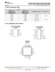
引脚图在P3P4P5P12Hot
典型应用电路图在P21P22
原理图在P11P12P14P15P17P18P22
封装尺寸在P37P38P39P40P41P42P43P45P46
标记信息在P37P38P39P40P41P42P43P44
封装信息在P36P37P38P39P40P41P42P43P44P45P46
技术参数、封装参数在P6
应用领域在P1P3P44P56
电气规格在P7P8
导航目录
UC3843D8数据手册
Page:
of 56 Go
若手册格式错乱,请下载阅览PDF原文件
6
UC1842
,
UC2842
,
UC3842
,
UC1843
,
UC2843
,
UC3843
UC1844
,
UC2844
,
UC3844
,
UC1845
,
UC2845
,
UC3845
SLUS223D –APRIL 1997–REVISED AUGUST 2016
www.ti.com
Product Folder Links: UC1842 UC2842 UC3842 UC1843 UC2843 UC3843 UC1844 UC2844 UC3844 UC1845
UC2845 UC3845
Submit Documentation Feedback Copyright © 1997–2016, Texas Instruments Incorporated
(1) Stresses beyond those listed under Absolute Maximum Ratings may cause permanent damage to the device. These are stress ratings
only, which do not imply functional operation of the device at these or any other conditions beyond those indicated under Recommended
Operating Conditions. Exposure to absolute-maximum-rated conditions for extended periods may affect device reliability.
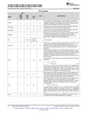
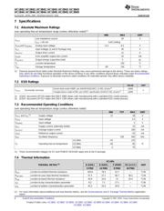
7 Specifications
7.1 Absolute Maximum Ratings
over operating free-air temperature range (unless otherwise noted)
(1)
MIN MAX UNIT
V
VCC
Low impedance source 30 V
I
VCC
< 30 mA Self Limiting
V
VFB
and V
ISENSE
Analog input voltage –0.3 6.3 V
V
VC
Input Voltage, Q and D Package only 30 V
I
OUTPUT
Output drive current ±1 A
I
COMP
Error amplifier output sink current 10 mA
E
OUTPUT
Output energy (capacitive load) 5 µJ
T
J
Junction temperature 150 °C
T
stg
Storage temperature –65 150 °C
(1) JEDEC document JEP155 states that 500-V HBM allows safe manufacturing with a standard ESD control process.
(2) JEDEC document JEP157 states that 250-V CDM allows safe manufacturing with a standard ESD control process.
7.2 ESD Ratings
VALUE UNIT
V
(ESD)
Electrostatic discharge
Human body model (HBM), per ANSI/ESDA/JEDEC JS-001, all pins
(1)
±3000
V
Charged device model (CDM), per JEDEC specification JESD22-C101, all pins
(2)
±3000
(1) These recommended voltages for VC and POWER GROUND apply only to the D package.
7.3 Recommended Operating Conditions
over operating free-air temperature range (unless otherwise noted)
MIN TYP MAX UNIT
V
VCC
and V
VC
(1)
Supply voltage 12 28 V
V
VFB
Input voltage 2.5 V
V
ISENSE
Input voltage 1 V
I
VCC
Supply current, externally limited 25 mA
I
OUTPUT
Average output current 200 mA
I
VREF
Reference output current –20 mA
f
OSC
Oscillator frequency 100 500 kHz
T
A
Operating free-air temperature
UC184x –55 125
°CUC284x –40 85
UC384x 0 70
(1) For more information about traditional and new thermal metrics, see the Semiconductor and IC Package Thermal Metrics application
report.
7.4 Thermal Information
THERMAL METRIC
(1)
UCx84x
UNITD (SOIC) D (SOIC) P (PDIP) FK (LCCC)
8 PINS 14 PINS 8 PINS 20 PINS
R
θJA
Junction-to-ambient thermal resistance 104.8 78.2 53.7 — °C/W
R
θJC(top)
Junction-to-case (top) thermal resistance 47.3 37.1 46.7 36.2 °C/W
R
θJB
Junction-to-board thermal resistance 45.9 32.6 31 35.4 °C/W
ψ
JT
Junction-to-top characterization parameter 8.2 7.3 17.1 — °C/W
ψ
JB
Junction-to-bottom characterization parameter 45.2 32.4 30.9 — ° C/W
器件 Datasheet 文档搜索
AiEMA 数据库涵盖高达 72,405,303 个元件的数据手册,每天更新 5,000 多个 PDF 文件
