Datasheet 搜索 > TI(德州仪器) > UCC27511DBV 数据手册 > UCC27511DBV 数据手册 1/24 页


¥ 0
UCC27511DBV 数据手册 - TI(德州仪器)
制造商:
TI(德州仪器)
描述:
单通道高速低侧栅极驱动器(具有4 -A峰值源和8 -A峰汇) Single-Channel High-Speed Low-Side Gate Driver (with 4-A Peak Source and 8-A Peak Sink)
Pictures:
3D模型
符号图
焊盘图
引脚图
产品图
页面导航:
典型应用电路图在P1P14
原理图在P8P15
封装尺寸在P19P20P21
型号编码规则在P2
封装信息在P2P3P19P20P21
功能描述在P13
技术参数、封装参数在P3
应用领域在P1P24
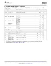
电气规格在P4P5P13P16
型号编号列表在P2P13
导航目录
UCC27511DBV数据手册
Page:
of 24 Go
若手册格式错乱,请下载阅览PDF原文件
1
2
3
5
4
EN
GND
IN+/IN-
VDD
OUT
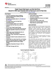
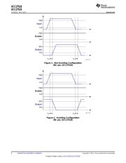
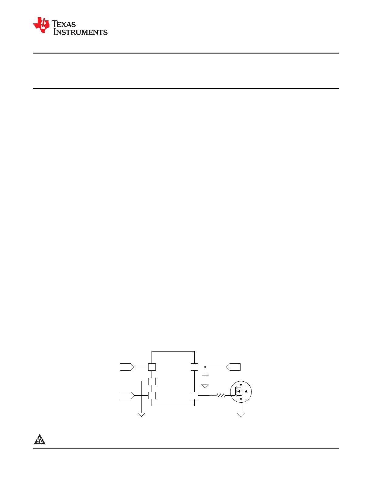
UCC27518/19
Q1
IN
4.5 V to 18 V
C1
R1
EN V+
UCC27518
UCC27519
www.ti.com
SLUSB33 –MAY 2012
Single Channel High-Speed, Low-Side Gate Driver
(Based On CMOS Input Threshold with 4-A Peak Source and 4-A Peak Sink)
Check for Samples: UCC27518 , UCC27519
1
FEATURES
APPLICATIONS
• Low-Cost, Gate-Driver Device Offering • Switch-Mode Power Supplies
Superior Replacement of NPN and PNP
• DC-to-DC Converters
Discrete Solutions
• Companion Gate Driver Devices for Digital
• Pin-to-Pin Compatible With TI's TPS2828 and
Power Controllers
the TPS2829
• Solar Power, Motor Control, UPS
• 4-A Peak Source and 4-A Peak Sink
• Gate Driver for Emerging Wide Band-Gap
Symmetrical Drive
Power Devices (such as GaN)
• Fast Propagation Delays (17-ns typical)
• Fast Rise and Fall Times (8-ns and 7-ns DESCRIPTION
typical)
The UCC27518 and UCC27519 single-channel, high-
speed, low-side gate driver device is capable of
• 4.5-V to 18-V Single Supply Range
effectively driving MOSFET and IGBT power
• Outputs Held Low During VDD UVLO (ensures
switches. Using a design that inherently minimizes
glitch free operation at power-up and power-
shoot-through current, UCC27518 and UCC27519
down)
are capable of sourcing and sinking high, peak-
• CMOS Input Logic Threshold (function of
current pulses into capacitive loads offering rail-to-rail
drive capability and extremely small propagation
supply voltage with hysteresis)
delay typically 17 ns.
• Hysteretic Logic Thresholds for High Noise
Immunity
The UCC27518 and UCC27519 provide 4-A source,
4-A sink (symmetrical drive) peak-drive current
• EN Pin for Enable Function (allowed to be no
capability at VDD = 12 V.
connect)
The UCC27518 and UCC27519 are designed to
• Output Held Low when Input Pins are Floating
operate over a wide VDD range of 4.5 V to 18 V and
• Input Pin Absolute Maximum Voltage Levels
wide temperature range of -40°C to 140°C. Internal
Not Restricted by VDD Pin Bias Supply
Under Voltage Lockout (UVLO) circuitry on VDD pin
Voltage
holds output low outside VDD operating range. The
• Operating Temperature Range of -40°C to
capability to operate at low voltage levels such as
140°C
below 5 V, along with best in class switching
characteristics, is especially suited for driving
• 5-Pin DBV Package (SOT-23)
emerging wide band-gap power switching devices
such as GaN power semiconductor devices.
Typical Application Diagrams
1
Please be aware that an important notice concerning availability, standard warranty, and use in critical applications of
Texas Instruments semiconductor products and disclaimers thereto appears at the end of this data sheet.
PRODUCTION DATA information is current as of publication date.
Copyright © 2012, Texas Instruments Incorporated
Products conform to specifications per the terms of the Texas
Instruments standard warranty. Production processing does not
necessarily include testing of all parameters.
器件 Datasheet 文档搜索
AiEMA 数据库涵盖高达 72,405,303 个元件的数据手册,每天更新 5,000 多个 PDF 文件
