Datasheet 搜索 > TI(德州仪器) > UCC27517A 数据手册 > UCC27517A 数据手册 1/31 页

¥ 0
UCC27517A 数据手册 - TI(德州仪器)
制造商:
TI(德州仪器)
描述:
具有 5V 负输入电压处理能力的 4A/4A 单通道高速低侧栅极驱动器
Pictures:
3D模型
符号图
焊盘图
引脚图
产品图
页面导航:
引脚图在P4Hot
典型应用电路图在P1P13P16P17
原理图在P12P13
封装尺寸在P25P27P28
标记信息在P25
封装信息在P4P24P25P26P27P28
功能描述在P11
技术参数、封装参数在P4
应用领域在P1P31
电气规格在P6P14
型号编号列表在P3
导航目录
UCC27517A数据手册
Page:
of 31 Go
若手册格式错乱,请下载阅览PDF原文件
1
2
3
5
4
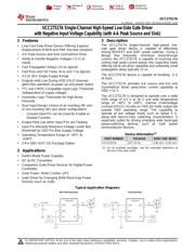
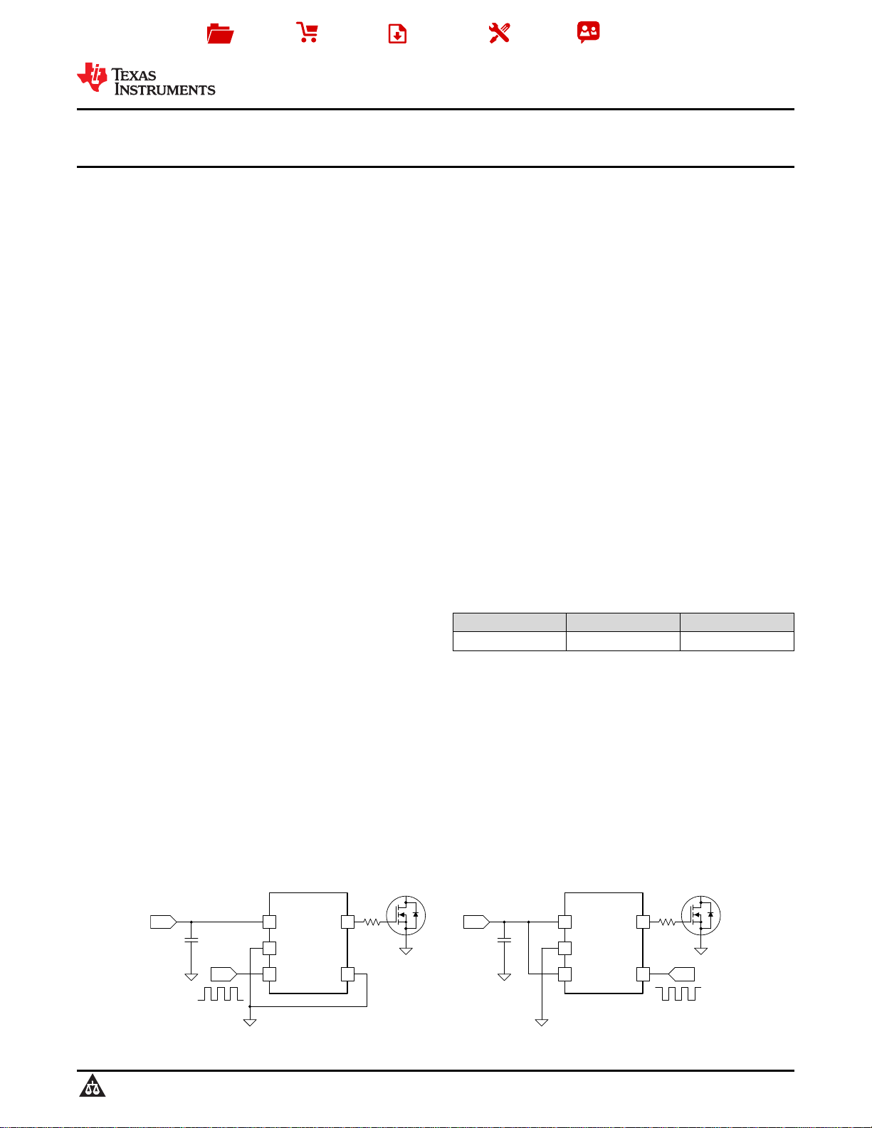
VDD
GND
IN+
OUT
IN-
UCC27517A
Q1
IN+
4.5 V to 18 V
Non-Inverting Input
V+
C1
R1
1
2
3
5
4
VDD
GND
IN+
OUT
IN-
UCC27517A
Inverting Input
VIN-
Q1
R1
4.5 V to 18 V
V+
C1
Product
Folder
Sample &
Buy
Technical
Documents
Tools &
Software
Support &
Community
UCC27517A
SLUSBQ0C – AUGUST 2013–REVISED AUGUST 2015
UCC27517A Single-Channel High-Speed Low-Side Gate Driver
with Negative Input Voltage Capability (with 4-A Peak Source and Sink)
1 Features 3 Description
The UCC27517A single-channel, high-speed, low-
1
• Low-Cost Gate-Driver Device Offering Superior
side gate driver device is capable of effectively
Replacement of NPN and PNP Discrete Solutions
driving MOSFET and IGBT power switches. Using a
• 4-A Peak-Source and Sink Symmetrical Drive
design that inherently minimizes shoot-through
• Ability to Handle Negative Voltages (-5 V) at
current, the UCC27517A is capable of sourcing and
sinking high peak-current pulses into capacitive loads
Inputs
offering rail-to-rail drive capability and extremely small
• Fast Propagation Delays (13-ns typical)
propagation delay typically 13 ns.
• Fast Rise and Fall Times (9-ns and 7-ns typical)
The UCC27517A device is capable of handling –5 V
• 4.5 to 18-V Single-Supply Range
at input.
• Outputs Held Low During VDD UVLO (ensures
The UCC27517A provides 4-A source and 4-A sink
glitch-free operation at power up and power down)
(symmetrical drive) peak-drive current capability at
• TTL and CMOS Compatible Input-Logic Threshold
VDD = 12 V.
(independent of supply voltage)
The UCC27517A is designed to operate over a wide
• Hysteretic-Logic Thresholds for High-Noise
VDD range of 4.5 V to 18 V and wide temperature
Immunity
range of –40°C to 140°C. Internal Undervoltage
• Dual Input Design (choice of an inverting (IN- pin)
Lockout (UVLO) circuitry on VDD pin holds output low
or non-inverting (IN+ pin) driver configuration)
outside VDD operating range. The capability to
operate at low voltage levels such as below 5 V,
– Unused Input Pin can be Used for Enable or
along with best-in-class switching characteristics, is
Disable Function
especially suited for driving emerging wide band-gap
• Output Held Low when Input Pins are Floating
power-switching devices such as GaN power
• Input Pin Absolute Maximum Voltage Levels Not
semiconductor devices.
Restricted by VDD Pin Bias Supply Voltage
Device Information
(1)
• Operating Temperature Range of –40°C to
PART NUMBER PACKAGE BODY SIZE (NOM)
+140°C
UCC27517A SOT-23 (5) 2.90 mm × 1.60 mm
• 5-Pin DBV (SOT-23) Package Option
(1) For all available packages, see the orderable addendum at
the end of the data sheet.
2 Applications
• Switch-Mode Power Supplies
• DC-to-DC Converters
• Companion Gate-Driver Devices for Digital-Power
Controllers
• Solar Power, Motor Control, UPS
• Gate Driver for Emerging Wide Band-Gap Power
Devices (such as GaN)
Typical Application Diagrams
1
An IMPORTANT NOTICE at the end of this data sheet addresses availability, warranty, changes, use in safety-critical applications,
intellectual property matters and other important disclaimers. PRODUCTION DATA.
器件 Datasheet 文档搜索
AiEMA 数据库涵盖高达 72,405,303 个元件的数据手册,每天更新 5,000 多个 PDF 文件
