Datasheet 搜索 > 稳压芯片 > TI(德州仪器) > UCC38085PWRG4 数据手册 > UCC38085PWRG4 数据手册 4/24 页
 器件3D模型
¥ 0
UCC38085PWRG4 数据手册 - TI(德州仪器)
制造商:
TI(德州仪器)
分类:
稳压芯片
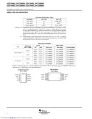
封装:
TSSOP-8
描述:
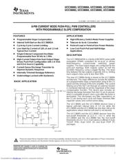
开关控制器 Crnt Mode Push-Pull w/Prog Slope Comp
Pictures:
3D模型
符号图
焊盘图
引脚图
产品图
页面导航:
导航目录
UCC38085PWRG4数据手册
Page:
of 24 Go
若手册格式错乱,请下载阅览PDF原文件
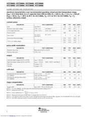
SLUS488B − SEPTEMBER 2002 − REVISED MAY 2003
4
www.ti.com
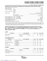
electrical characteristics over recommended operating virtual junction temperature range,
V
DD
= 10 V (See Note 1),1-µF capacitor from VDD to GND, R
T
= 165 kΩ, R
F
= 1 kΩ, C
F
= 220 pF,
R
SET
= 50 kΩ, T
A
= −40°C to 85°C for UCC2808x, T
A
= 0°C to 70°C for UCC3808x, T
A
= T
J
(unless otherwise noted)
current sense
PARAMETER TEST CONDITIONS MIN TYP MAX UNITS
Gain See Note 3 1.9 2.2 2.5 V/V
Maximum input signal voltage CTRL = 5 V, See Note 4 0.47 0.52 0.57 V
CS to output delay time CTRL = 3.5 V, 0 mV ≤ CS ≤ 600 mV 100 200 ns
Source current −200 nA
Sink current
CS = 0.5 V, RT = 2.0 V,
See Note 5
3 7 12 mA
Overcurrent threshold voltage 0.70 0.75 0.80 V
CTRL to CS offset voltage
CS = 0 V, 25°C 0.55 0.70 0.90 V
CTRL to CS offset voltage
CS = 0 V 0.37 0.70 1.10 V
pulse width modulation
PARAMETER TEST CONDITIONS MIN TYP MAX UNITS
Maximum duty cycle Measured at OUTA or OUTB 48% 49% 50%
Minimum duty cycle CTRL = 0 V 0%
output
PARAMETER TEST CONDITIONS MIN TYP MAX UNITS
Low-level output voltage (OUTA or OUTB) I
OUT
= 100 mA 0.5 1.0
V
High-level output voltage (OUTA or OUTB) I
OUT
= −50 mA, (VDD − VOUT), See Note 6 0.5 1.0
V
Rise time C
LOAD
= 1 nF 25 60
ns
Fall time C
LOAD
= 1 nF 25 60
ns
soft-start
PARAMETER TEST CONDITIONS MIN TYP MAX UNITS
OUTA/OUTB soft-start interval time,
UCC38083/4
CTRL = 1.8 V, CS = 0 V,
Duty cycle from 0 to full
1.3 3.5 8.5 ms
OUTA/OUTB soft-start interval time,
UCC38085/6
CTRL = 1.8 V, CS = 0 V,
Duty cycle from 0 to full
30 75 110 µs
slope compensation
PARAMETER TEST CONDITIONS MIN TYP MAX UNITS
I
RAMP
, peak I
SET
, peak = 30 µA,Full duty cycle 125 150 175 µA
NOTE 1: For UCCx8083/5, set VDD above the start threshold before setting to 10 V.
NOTE 2: Measured at ISET pin.
NOTE 3: Gain is defined by A +
DV
CTRL
DV
CS
, 0 ≤ V
CS
≤ 0.4 V.
NOTE 4: Measured at trip point of latch with CS ramped from 0.4 V to 0.6 V.
NOTE 5: This internal current sink on the CS pin is designed to discharge and external filter capacitor. It is not intended to be a dc sink path.
NOTE 6: Not 100% production tested. Ensured by design and also by the rise time test.
Downloaded from Elcodis.com electronic components distributor
器件 Datasheet 文档搜索
AiEMA 数据库涵盖高达 72,405,303 个元件的数据手册,每天更新 5,000 多个 PDF 文件
